


388 AMD Geode™ SC1200/SC1201 Processor Data Book
Electrical Specifications
32579B
9.3.6 PCI Bus
The SC1200/SC1201 processor is compliant with PCI bus
v2.1 specification. Relevant information from the PCI bus
specification is provided below.
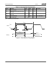
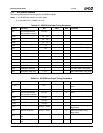
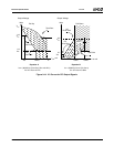
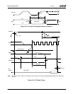
All parameters in Table 9-20 are not 100% tested. The
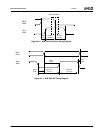
parameters in this table are further described in Figure 9-
14.
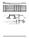
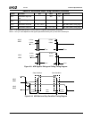
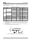
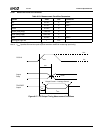
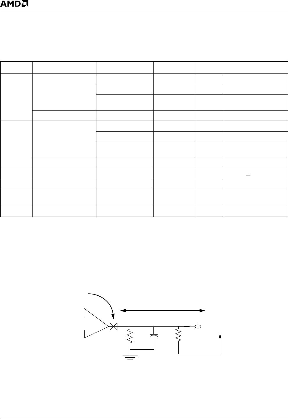
Figure 9-13. Testing Setup for PCI Slew Rate and Minimum Timing
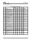
Table 9-20. PCI AC Specifications
Symbol Parameter Min Max Unit Comments
I
OH
(AC)
(Note 1)
Switching current high -12V
IO
mA 0 < V
OUT
≤ 0.3V
IO,
-17.1(V
IO
-V
OUT
)mA0.3V
IO
< V
OUT
< 0.9V
IO
Equation A
(Figure 9-14)
0.7V
IO
< V
OUT
< V
IO
Test point (Note 2) -32V
IO
mA V
OUT
= 0.7V
IO
I
OL
(AC)
(Note 1)
Switching current low 16V
IO
mA V
IO
> V
OUT
≥ 0.6V
IO
26.7V
OUT
mA 0.6V
IO
> V
OUT
> 0.1V
IO
Equation B
(Figure 9-14)
0.18V
IO
>V
OUT
>0
Test point (Note 2) 38V
IO
mA V
OUT
= 0.18V
IO
I
CL
Low clamp current -25+(V
IN
+1)/0.015 mA -3 < V
IN
< -1
I
CH
High clamp current 25+(V
IN
-V
IO
-1)/0.015 mA V
IO
+4 > V
IN
> V
IO
+1
SLEW
R
(Note 3)
Output rise slew rate 1 4 V/ns 0.2V
IO
- 0.6V
IO
Load
SLEW
F
Output fall slew rate 1 4 V/ns 0.6V
IO
- 0.2V
IO
Load
Note 1. Refer to the V/I curves in Figure 9-14. This specification does not apply to PCICLK0, PCICLK1, and PCIRST# which
are system outputs.
Note 2. Maximum current requirements are met when drivers pull beyond the first step voltage. Equations which define
these maximum values (A and B) are provided with relevant diagrams in Figure 9-14. These maximum values are
guaranteed by design.
Note 3. Rise slew rate does not apply to open-drain outputs. This parameter is interpreted as the cumulative edge rate
across the specified range, according to the test circuit in Figure 9-13.
Buffer
V
CC
0.5" max.
Pin
1 K
Ω1 KΩ 10 pF
Output