AMD Geode™ SC1200/SC1201 Processor Data Book 237
Core Logic Module - SMI Status and ACPI Registers - Function 1
32579B
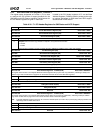
6.4.2.1 SMI Status Support Registers
F1 Index 10h, Base Address Register 0 (F1BAR0), points
to the base address for SMI Status register locations. Table
6-33 gives the bit formats of I/O mapped SMI Status regis-
ters accessed through F1BAR0.
The registers at F1BAR0+I/O Offset 50h-FFh can also be
accessed F0 Index 50h-FFh. The preferred method is to
program these registers through the F0 register space.
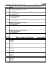
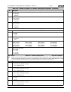
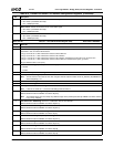
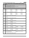
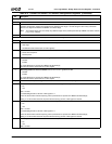
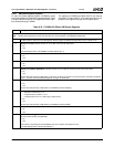
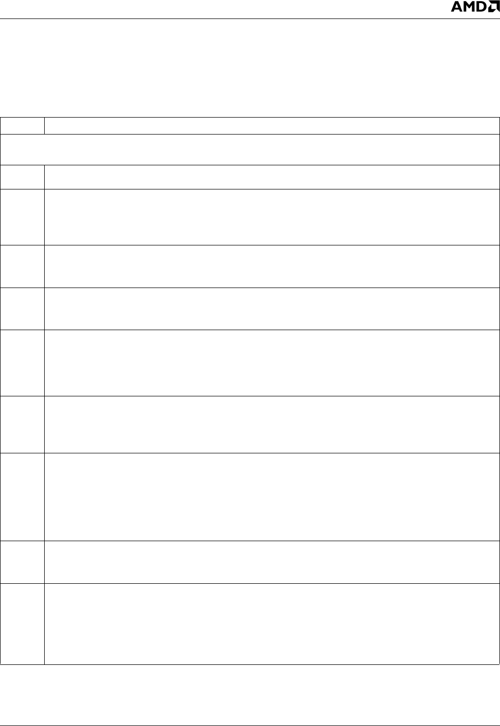
Table 6-33. F1BAR0+I/O Offset: SMI Status Registers
Bit Description
Offset 00h-01h Top Level PME/SMI Status Mirror Register (RO) Reset Value: 0000h
Note: Reading this register does not clear the status bits. For more information, see F1BAR0+I/O Offset 02h.
15 Suspend Modulation Enable Mirror. This bit mirrors the Suspend Mode Configuration bit (F0 Index 96h[0]). It is used by
the SMI handler to determine if the SMI Speedup Disable Register (F1BAR0+I/O Offset 08h) must be cleared on exit.
14 SMI Source is USB. Indicates whether or not an SMI was caused by USB activity
0: No.
1: Yes.
To enable SMI generation, set F5BAR0+I/O Offset 00h[20:19] to 11.
13 SMI Source is Warm Reset Command. Indicates whether or not an SMI was caused by a Warm Reset command.
0: No.
1: Yes.
12 SMI Source is NMI. Indicates whether or not an SMI was caused by NMI activity.
0: No.
1: Yes.
11 SMI Source is IRQ2 of SIO Module. Indicates whether or not an SMI was caused by IRQ2 of the SIO module.
0: No.
1: Yes.
The next level (second level) of SMI status is reported in the SuperI/O module. For more information, see Table 5-29 "Banks
0 and 1 - Common Control and Status Registers" on page 118, Offset 00h.
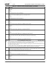
10 SMI Source is EXT_SMI[7:0]. Indicates whether or not an SMI was caused by a negative-edge event on EXT_SMI[7:0].
0: No.
1: Yes.
The next level (second level) of SMI status is at F1BAR0+I/O Offset 24h[23:8].
9 SMI Source is GP Timers/UDEF/PCI/ISA Function Trap. Indicates if an SMI was caused by:
— Expiration of GP Timer 1 or 2.
— Trapped access to UDEF1, 2, or 3.
— Trapped access to F1-F5 or ISA Legacy register space.
0: No.
1: Yes.
The next level (second level) of SMI status is at F1BAR0+I/O Offset 04h/06h.
8 SMI Source is Software Generated. Indicates whether or not an SMI was caused by software.
0: No.
1: Yes.
7 SMI on an A20M# Toggle. Indicates whether or not an SMI was caused by a write access to either Port 92h or the keyboard
command which initiates an A20M# SMI.
0: No.
1: Yes.
This method of controlling the internal A20M# in the GX1 module is used instead of a pin.
To enable SMI generation, set F0 Index 53h[0] to 1.


