AMD Geode™ SC1200/SC1201 Processor Data Book 405
Electrical Specifications
32579B
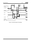
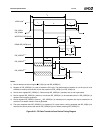
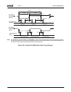
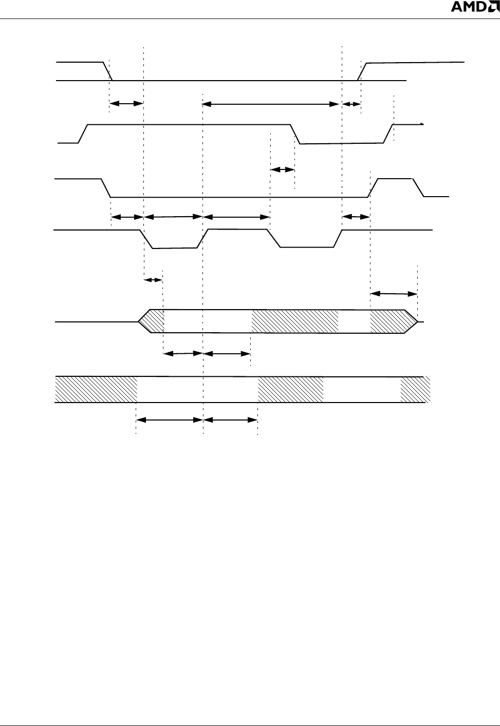
Figure 9-27. Multiword DMA Data Transfer Timing Diagram
t
M
t
N
t
L
t
j
t
K
t
D
t
I
t
E
t
Z
t
F
t
G
t
G
t
H
t
0
IDE_CS[1:0]#
IDE_DATA[15:0]
IDE_DATA[15:0]
IDE_DREQ0
IDE_DACK0#
IDE_IOR0#
IDE_IOW0#
Notes:
1) For Multiword DMA transfers, the Device may negate IDE_DREQ[0:1] within the tL specified time once IDE_DACK[0:1
is asserted, and reassert it again at a later time to resume the DMA operation. Alternatively, if the device is able to c
o
tinue the transfer of data, the device may leave IDE_DREQ[0:1] asserted and wait for the host to reass
e
IDE_DACK[0:1]#.
2) This signal can be negated by the host to Suspend the DMA transfer in process.


