


57
CHAPTER 5 PRECAUTIONARY INFORMATION FOR THE FR FAMILY CPU
■ Interlocking
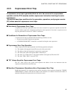
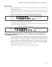
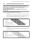
Instructions which are relatively slow in loading data to the CPU may cause register hazards that cannot be
handled by register bypassing.
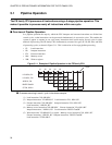
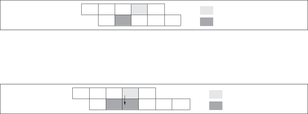
In the example in Figure 5.3-3, data required for the "ID" stage of the "SUB" instruction must be loaded to
the CPU in the "MA" stage of the "LD" instruction, creating a hazard that cannot be avoided by the bypass
function.
Figure 5.3-3 Example: Register Hazard that Cannot be Avoided by Bypassing
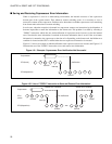
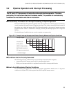
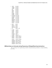
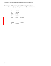
In cases such as this, the FR family CPU executes the instruction correctly by pausing before execution of
the subsequent instruction. This function is called interlocking.
In the example in Figure 5.3-4, the "ID" stage of the "SUB" instruction is delayed until the data is loaded
from the "MA" stage of the "LD" instruction.
Figure 5.3-4 Example of Interlocking
■ Interlocking Produced by Reference to "R15" and General-purpose Registers after
Changing the "S" Flag
The general-purpose register "R15" is designed to function as either the system stack pointer (SSP) or user
stack pointer (USP). For this reason, the FR family CPU is designed to automatically generate an interlock
whenever a change to the "S" flag in the condition code register (CCR) in the program status (PS) is
followed immediately by an instruction that references the "R15". This interlock enables the CPU to
reference the "SSP" or "USP" values in the order in which they are written in the program. FR family
hardware design similarly generates an interlock whenever a TYPE-A format instruction immediately
follows an instruction that changes the value of the "S" flag.
For information on instruction format types, see Section "6.1 Instruction Formats".
IF ID EX MA WB : Data read cycle to R0
: Read cycle from R1
IF ID EX MA WBSUB R1, R2
LD @R0, R1
IF ID EX MA WB : Data read cycle to R0
: Read cycle from R1
IF ID ID MAEX WBSUB R1, R2
LD @R0, R1