


www.ti.com
PRODUCT PREVIEW
TMS320C6454
Fixed-PointDigitalSignalProcessor
SPRS311A–APRIL2006–REVISEDDECEMBER2006
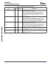
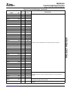
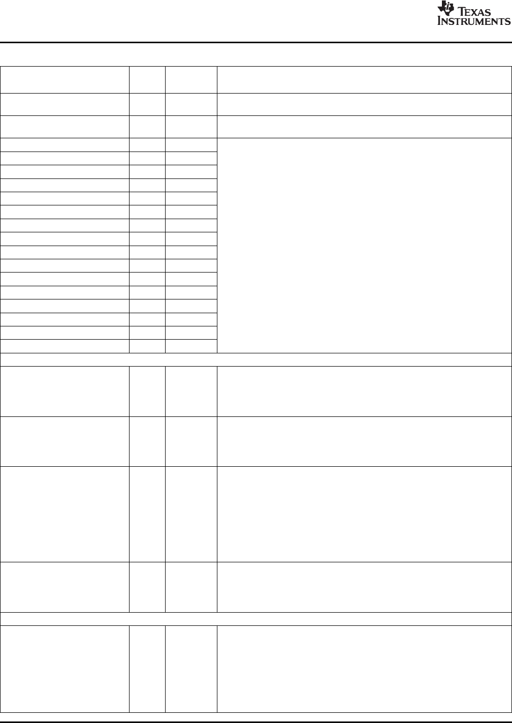
Table2-3.TerminalFunctions(continued)
SIGNAL
TYPE
(1)
IPD/IPU
(2)
DESCRIPTION
NAMENO.
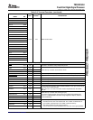
Reserved.Thispinmustbeconnectedtothe1.8-VI/Osupply(DV
DD18
)viaa
RSV34E6
1-kΩresistorforproperdeviceoperation.
Reserved.Thispinmustbeconnecteddirectlytogroundforproperdevice
RSV35D6
operation.
RSV63AD20I
RSV64AC15I
RSV65AC17I
RSV66AD16I
RSV67U16I
RSV68V15I
RSV69V17I
RSV70W16I
Reserved.ThesepinsmustbeconnecteddirectlytoV
SS
forproperdevice
operation.
RSV71W18I
RSV72AE17I
RSV73AE19I
RSV74AE23I
RSV75AF20I
RSV76AH20I
RSV77AJ17I
RSV78AJ23I
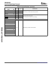
SUPPLYVOLTAGEMONITORPINS
Die-side1.2-Vcoresupply(CV
DD
)voltagemonitorpin.Themonitorpins
indicatethevoltageonthedieand,therefore,providethebestprobepointfor
CV
DDMON
N1voltagemonitoringpurposes.Formoreinformationregardingtheuseofthis
andothervoltagemonitoringpins.IftheCV
DDMON
pinisnotused,itshouldbe
connecteddirectlytothe1.2-Vcoresupply(CV
DD
).
Die-side3.3-VI/Osupply(DV
DD33
)voltagemonitorpin.Themonitorpins
indicatethevoltageonthedieand,therefore,providethebestprobepointfor
DV
DD33MON
L6voltagemonitoringpurposes.Formoreinformationregardingtheuseofthis
andothervoltagemonitoringpins.IftheDV
DD33MON
pinisnotused,itshould
beconnecteddirectlytothe3.3-VI/Osupply(DV
DD33
).
Die-side1.5-/1.8-VI/Osupply(DV
DD15
)voltagemonitorpin.Themonitorpins
indicatethevoltageonthedieand,therefore,providethebestprobepointfor
voltagemonitoringpurposes.Formoreinformationregardingtheuseofthis
andothervoltagemonitoringpins.IftheDV
DD15MON
pinisnotused,itshould
beconnecteddirectlytothe1.5-/1.8-VI/Osupply(DV
DD15
).
DV
DD15MON
F3I
NOTE:IftheRGMIImodeoftheEMACisnotused,theDV
DD15
,DV
DD15MON
,
V
REFHSTL
,RSV13,andRSV14pinscanbeconnecteddirectlytoground(V
SS
)
tosavepower.However,connectingthesepinsdirectlytogroundwillprevent
boundary-scanfromfunctioningontheRGMIIpinsoftheEMAC.Topreserve
boundary-scanfunctionalityontheRGMIIpins,seeSection7.3.4.
Die-side1.8-VI/Osupply(DV
DD18
)voltagemonitorpin.Themonitorpins
indicatethevoltageonthedieand,therefore,providethebestprobepointfor
DV
DD18MON
A26voltagemonitoringpurposes.Formoreinformationregardingtheuseofthis
andothervoltagemonitoringpins.IftheDV
DD18MON
pinisnotused,itshould
beconnecteddirectlytothe1.8-VI/Osupply(DV
DD18
).
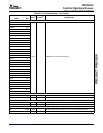
SUPPLYVOLTAGEPINS
(DV
DD18
/2)-VreferenceforSSTLbuffer(DDR2MemoryController).Thisinput
voltagecanbegenerateddirectlyfromDV
DD18
usingtwo1-kΩresistorstoform
aresistordividercircuit.
NOTE:TheDDR2MemoryControllerisnotused,theV
REFSSTL
,RSV11,and
V
REFSSTL
C14ARSV12pinscanbeconnecteddirectlytoground(V
SS
)tosavepower.
However,connectingthesepinsdirectlytogroundwillpreventboundary-scan
fromfunctioningontheDDR2MemoryControllerpins.Topreserve
boundary-scanfunctionalityontheDDR2MemoryControllerpins,see
Section7.3.4.
DeviceOverview 38SubmitDocumentationFeedback