


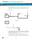
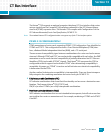
CT Bus Interface: Katana®752i CT Bus Options
Katana
®
752i User’s Manual 10006024-04
13-2
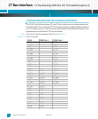
• User Managed Combination (UMC)
UMC indicates combinations that are not to be made casually, since they may not be com-
patible. Potential device destruction must be assumed for these combinations. For exam-
ple, a PMC64 combined with a PT3CC is subject to damage from incompatible signal
mapping on Pn3/Jn3.
Caution: Do not install 64-bit PMC cards on the Katana
®
752i since this is an invalid configuration
and would cause possible damage.
For a list of these combinations, refer to the compatibility matrix in the PCI Telecom Mezza-
nine/Carrier Card Specification, PICMG 2.15.
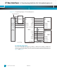
KATANA
®
752I CT BUS OPTIONS
Two Katana
®
752i CT bus options are available:
• Option 1
(See page 13-4)
This option supports only CT clocks—C8A, C8B, FRAMEA, FRAMEB, NETREF1, and NETREF2
between the J4 connector and PTMC sites. There is no data path between the J4 and PTMC
sites. There is an 8-bit data path between the two PTMC sites with this option, see
Fig. 13-2.
• Option 2
(See page 13-6)
This option supports CT bus clocking plus CT data traffic via an Agere Systems T8110 Time
Slot Interchanger (TSI). See
Fig. 13-3 for data connectivity between J4 and the two PTMC
sites.
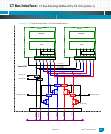
CLOCKING
In a typical system clocking model, the designated primary clock master drives the A clock
and frame signals and the designated secondary master drives the B clock and frame sig-
nals. In
Fig. 13-1, initially the B clocks are locked to the A clocks. After fallback, the roles of
the A and B clocks are reversed. For example, the board driving the B clocks becomes the
primary master after the A clock source fails. The NETFREF signals are generated to the pri-
mary master to provide a network reference that the primary master will use to synchronize
clock A with the network reference.
!