Overview: Functional Overview
Katana®752i User’s Manual 10006024-04
1-4
FUNCTIONAL OVERVIEW
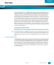
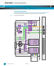
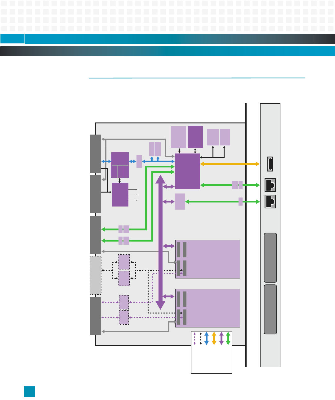
The following block diagram provides a functional overview for the Katana®752i.
Figure 1-1: General System Block Diagram
J1 J2
J3 cPSB& I/O
Marvell
D-III
System
Controller
32/64/128
MB Flash
256/512MB
1GB/2GB
DDR SDRAM
512KB
Socketed
Flash
PMC Site #1
32 bit/33/66MHz PCI
64 User I/O
CT Bus per PT2MC
PMC Site #2
32 bit/33/66MHz PCI
64 User I/O
CT Bus per PT2MC
Opt J4 H.110 J5 I/O
RS232
μDB-9
RJ45
1000BaseT
CT Bus Clocks
User I/O
User I/O
NVRAM
IPMI
CTRL
FRU ROM
Voltage
Monitors
Temp
Sensors
Power Supply
& Monitoring
Switch
BCM
5461S
MAG
RTC
BCM
5461S
MAG
IBM
750GX
BCM
5461S
MAG
RJ45
1000BaseT
MAG
GbE
MAC/PHY
GMII
Clock
Buffer
Opt. TSI
T8110
PCI
Opt.
KS8721CL
Opt.
KS8721CL
J12
J11
J13
J22
J21 J23
J24
J14
RMII
RMII
3.3V
2.5V
1.5V
PCI
RS232
1000BaseT
I
2
C
CT Bus
CPCI
Power
PTMC Ethernet


