


CT Bus Interface: Signal Control
10006024-04 Katana
®
752i User’s Manual
13-3
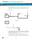
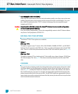
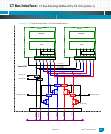
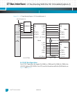
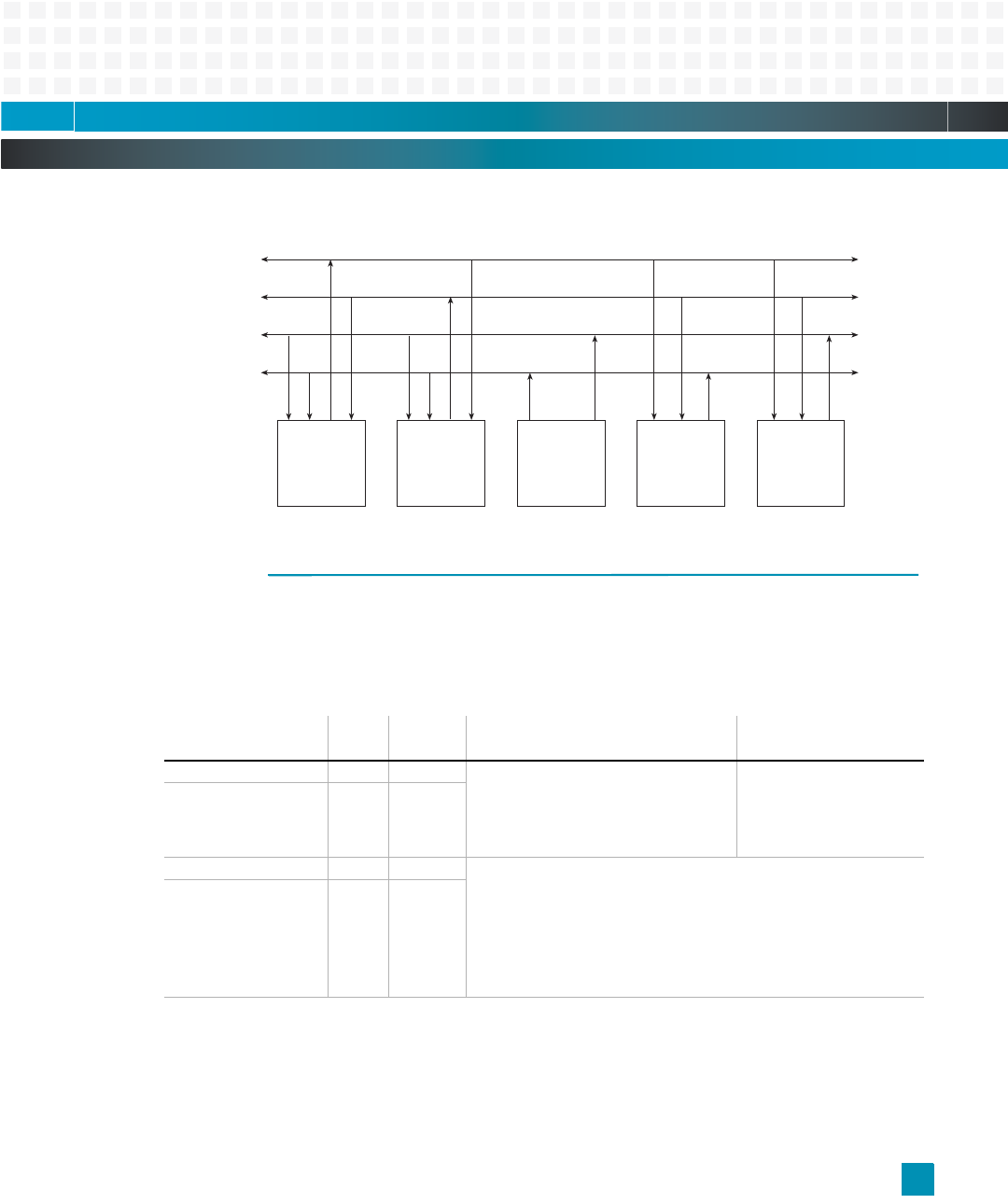
Figure 13-1: Typical System Clocking Model
SIGNAL CONTROL
The Katana
®
752i supports control signals that allow a PTMC site to master the CT clocks
and/or data. The control registers are located in the Hot Swap Logic (HSL) programmable
logic device (PLD) at hex address F821,0003
16
. The 750GL processor can access these reg-
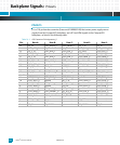
isters. The following table summarizes the direction control registers:
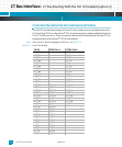
Table 13-1: CT Clock Control Registers
Register: Bit:
Reset
Value:
T8110 Not Installed
(option 1):
T8110 Installed
(option 2):
NETREF1_DIR 0 1 Controls direction of NETREF (on J4):
1=Katana
®
752i is NETREFx slave
(input)
0=Katana
®
752i is NETREFx master
(output)
These bits are not used.
NETREF2_DIR 1 1
C8_FRAME_A_TERM 2 1 Controls termination of FRAME and C8 data signals (on J4):
1=Katana
®
752i is not clock master (33 ohm series
termination)
0=Katana
®
752i is clock master (no series termination)
Controls termination on clock signals:
1=33-ohm series termination present
0=no termination
C8_FRAME_B_TERM 3 1
Primary
Master
Secondary
Master
Bits
Derived
Source
Slave
Digital
Trunk
Card
Slave
Digital
Trunk
Card
CT_C8_A/CT_FRAME_A
CT_C8_B/CT_FRAME_B
CT_NETREF_1
CT_NETREF_2