


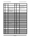
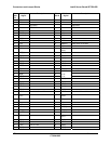
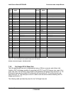
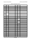
Intel® Server Board SE7520JR2 Connectors and Jumper Blocks
Revision 1.0
C78844-002
177
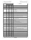
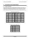
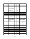
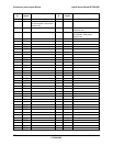
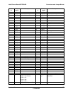
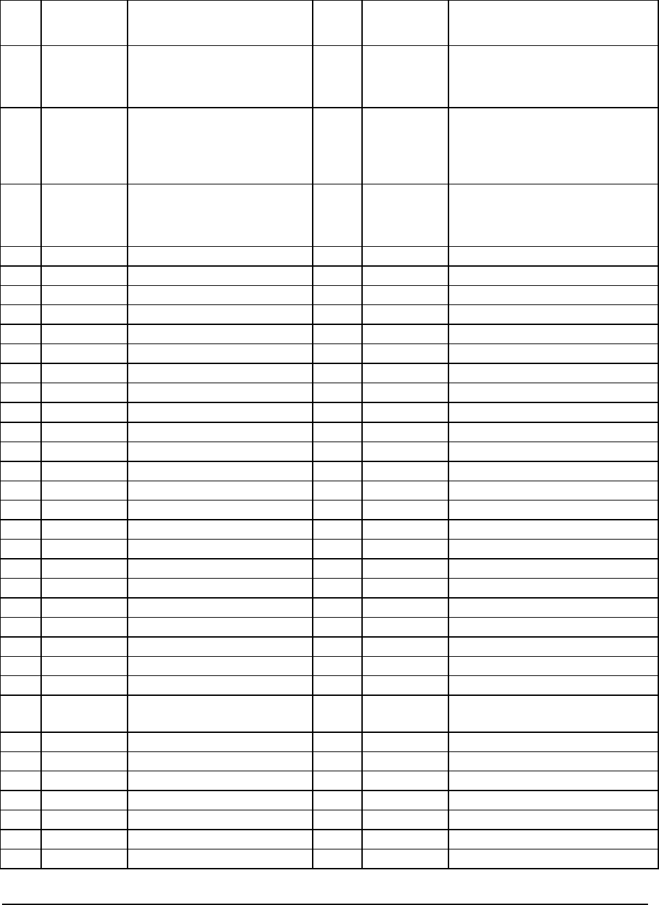
Pin-
Side
B
PCI Spec
Signal
Description Pin-
Side A
PCI Spec
Signal
Description
96 +5V 96 INTA# This pin will be connected on the 2U
riser to INT_A# of the bottom PCI
slot, INT_D# of the middle slot and
INT_C# of the top slot.
95 INTB# This pin will be connected on
the 2U riser to INT_B# of the
bottom PCI slot, INT_A# of the
middle slot and INT_D# of the
top slot.
95 INTC# This pin will be used by 1U/2U riser
to bring the INT_C# interrupt on the
bottom PCI slot down to the
baseboard.
94 INTD# This pin will be used by 1U/2U
riser to bring the INT_D#
interrupt on the bottom PCI slot
down to the baseboard.
94 +5V
93 +5V 93 GND
92 GND 92 REQ3# Highest PCI Slot (SLOT3)
91 CLK3 Highest PCI Slot (SLOT3) 91 GND
90 GND 90 GNT3# Highest PCI Slot (SLOT3)
89 CLK2 Middle PCI Slot (SLOT2) 89 +5V Was GND
88 GND 88 RSVD
87 REQ2# Middle PCI Slot (SLOT2) 87 +5V Was GND
86 GND 86 LECC4
85 LECC5 85 GND Was Vio 3.3V or 1.5V
84 GND 84 LECC3
83 +3.3V 83 GNT2#
82 LECC2 82 3.3VAUX 3 slots at 375ma
81 GND 81 RST#
80 CLK1 Lowest PCI slot (SLOT1) 80 +3.3V Was VIO 3.3V or 1.5V
79 GND 79 GNT1# Lowest PCI slot (SLOT1)
78 REQ1# Lowest PCI slot (SLOT1) 78 GND
77 +3.3V Was 3.3V or 1.5V 77 PME#
76 AD[31] 76 AD[30]
75 AD[29] 75 +3.3V
74 GND 74 AD[28]
73 AD[27] 73 AD[26]
72 AD[25] 72 GND
71 +3.3V 71 AD[24]
70 C/BE[3]# 70 RSVD
Lower slot IDSEL=AD17 Middle
Slot=AD18, Top slot=AD19
69 AD[23] 69 +3.3V
68 GND 68 AD[22]
67 AD[21] 67 AD[20]
66 AD[19] 66 GND
65 +3.3V 65 AD[18]
64 AD[17] 64 AD[16]
63 C/BE[2]# 63 +3.3V