


Connectors and Jumper Blocks Intel® Server Board SE7520JR2
Revision 1.0
C78844-002
194
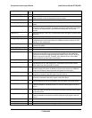
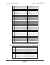
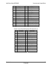
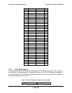
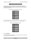
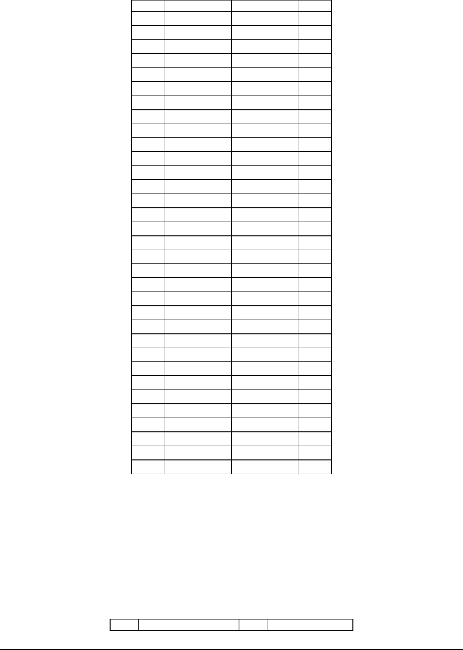
Pin# Signal Name Signal Name Pin#
2 +DB(13) -DB(13) 36
3 +DB(14) -DB(14) 37
4 +DB(15) -DB(15) 38
5 +DB(P1) -DB(P1) 39
6 +DB(0) -DB(0) 40
7 +DB(1) -DB(1) 41
8 +DB(2) -DB(2) 42
9 +DB(3) -DB(3) 43
10 +DB(4) -DB(4) 44
11 +DB(5) -DB(5) 45
12 +DB(6) -DB(6) 46
13 +DB(7) -DB(7) 47
14 +DB(P) -DB(P) 48
15 GROUND GROUND 49
16 GROUND GROUND 50
17 RESERVED RESERVED 51
18 RESERVED RESERVED 52
19 RESERVED RESERVED 53
20 GROUND GROUND 54
21 +ATN -ATN 55
22 GROUND GROUND 56
23 +BSY -BSY 57
24 +ACK -ACK 58
25 +RST -RST 59
26 +MSG -MSG 60
27 +SEL -SEL 61
28 +C/D -C/D 62
29 +REQ -REQ 63
30 +I/O -I/O 64
31 +DB(8) -DB(8) 65
32 +DB(9) -DB(9) 66
33 +DB(10) -DB(10) 67
34 +DB(11) -DB(11) 68
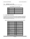
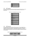
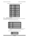
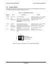
7.5.4 ATA-100 Connector
The Server Board SE7520JR2 provides one legacy ATA-100 40-pin connector (J3K1). The pin-
out is defined in the following table. Its signals are not tied to the ATA functionality embedded
into the high-density 100-pin front panel connector. Each connector is configured to a separate
ATA port embedded in the ICH5-R.
Table 97: ATA-100 40-pin Connector Pin-out (J3K1)
Pin Signal Name Pin Signal Name