


Intel® Server Board SE7520JR2 Connectors and Jumper Blocks
Revision 1.0
C78844-002
181
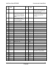
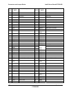
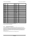
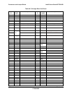
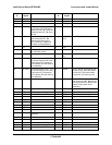
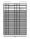
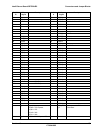
Pin-Side
B
PCI Spec
Signal
Description Pin-Side
A
PCI Spec
Signal
Description
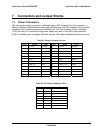
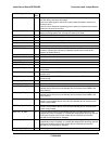
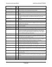
101 HSOn(7) 101 GND
100 GND 100 HSIp(7)
99 +5V 99 HSIn(7)
98 INTB# This pin will be connected on
the 2U riser to INT_B# of the
bottom PCI slot, INT_A# of the
middle slot and INT_D# of the
top slot.
98 GND
97 INTD# This pin will be used by 1U/2U
riser to bring the INT_B#
interrupt from the top and
INT_C# from the middle PCI
slot down to the baseboard.
97 ZCR_PRS
NT_L
From TDI of lowest slot only
96 +5V 96 +5V
95 Reserved SLOT_ID_FL, not required as
the risers are unique.
95 +5V
94 +5V 94 ZCR_MSKI
D_L
From TMS of lowest slot only
93 IOP INTA SCSI Interrupt A to ZCR. This
pin will be used by 1U/2U riser
to bring the INT_C# interrupt
on the bottom PCI slot down to
the baseboard
93 +5V
92 IOP INTB SCSI Interrupt B to ZCR. This
pin will be used by 1U/2U riser
to bring the INT_D# interrupt
on the bottom PCI slot down to
the baseboard
92 INTA# This pin will be connected on the
2U riser to INT_A# of the bottom
PCI slot, INT_D# of the middle
slot and INT_C# of the top slot.
91 GND 91 INTC# This pin will be used by 1U/2U
riser to bring the INT_A# interrupt
from the top and INT_B# from the
middle PCI slot down to the
baseboard.
90 CLK3 Highest PCI Slot (SLOT3) 90 GND
89 GND 89 REQ3# Highest PCI Slot (SLOT3)
88 CLK2 Middle PCI Slot (SLOT2) 88 GND
87 GND 87 GNT3# Highest PCI Slot (SLOT3)
86 REQ2# Middle PCI Slot (SLOT2) 86 GND
85 GND 85 RST#
84 Reserved 84 GND
83 GND 83 Reserved
KEY KEY
KEY End of x16 PCI-Express
connector
KEY
82 Reserved 82 +5V Was Vio 3.3V or 1.5V
81 GND 81 Reserved
80 CLK1 Lowest PCI slot (SLOT1) 80 GND
79 Ground 79 GNT2# Middle PCI Slot (SLOT2)
78 REQ1# Lowest PCI slot (SLOT1) 78 +3.3V Was Vio 3.3V or 1.5V