


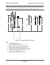
Intel® Server Board SE7520JR2 Design and Environmental Specifications
Revision 1.0
C78844-002
207
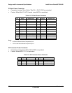
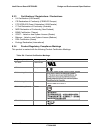
8.2.5 Voltage Regulation
The power supply output voltages must stay within the following voltage limits when operating at
steady state and dynamic loading conditions. These limits include the peak-peak ripple/noise.
All outputs are measured with reference to the return remote sense signal (ReturnS). The 5V,
12V1, 12V2, +12V3, –12V and 5VSB outputs are measured at the power supply connectors
referenced to ReturnS. The +3.3V is measured at it remote sense signal (3.3VS) located at the
signal connector.
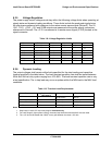
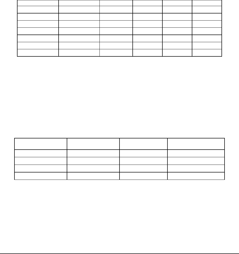
Table 118: Voltage Regulation Limits
Parameter Tolerance Minimum Nominal Maximum Units
+ 3.3V - 5% / +5% +3.14 +3.30 +3.46 V
rms
+ 5V - 5% / +5% +4.75 +5.00 +5.25 V
rms
+ 12V1 - 5% / +5% +11.40 +12.00 +12.60 V
rms
+ 12V2 - 5% / +5% +11.40 +12.00 +12.60 V
rms
+ 12V3 - 5% / +5% +11.40 +12.00 +12.60 V
rms
- 12V - 5% / +9% -11.40 -12.00 -13.08 V
rms
+ 5VSB - 5% / +5% +4.75 +5.00 +5.25 V
rms
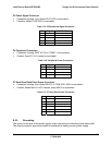
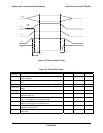
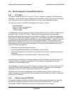
8.2.6 Dynamic Loading
The output voltages shall remain within limits specified for the step loading and capacitive
loading specified in the table below. The load transient repetition rate shall be tested between
50Hz and 5kHz at duty cycles ranging from 10%-90%. The load transient repetition rate is only
a test specification. The ∆ step load may occur anywhere within the MIN load to the MAX load
conditions.
Table 119: Transient Load Requirements
Output
∆ Step Load Size
(See note 2)
Load Slew Rate Test Capacitive Load
+3.3V 5.0A
0.25 A/µsec 250 µF
+5V 4.0A
0.25 A/µsec 400 µF
12V1+12V2+12V3 20.0A
0.25 A/µsec 2200 µF
1, 3
+5VSB 0.5A
0.25 A/µsec 20 µF
Notes
1. Step loads on each 12V output may happen simultaneously.
2. For Load Range 2 (light system loading), the tested step load size should be 60% of those listed.
3. The +12V should be tested with 1000µF evenly split between the three +12V rails.