


122 Rabbit 3000 Microprocessor
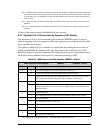
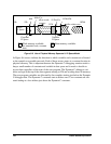
The Memory Timing Control Register (MTCR) enables the extended timing for the memory
output enables and write enables. See Figure 7-2 for details on how the timing of the mem-
ory read and write strobes is affected when using the early output enable and write enable
options. Figure 16-3 shows extended output enable and write enable timing diagrams.
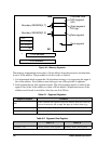
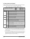
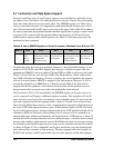
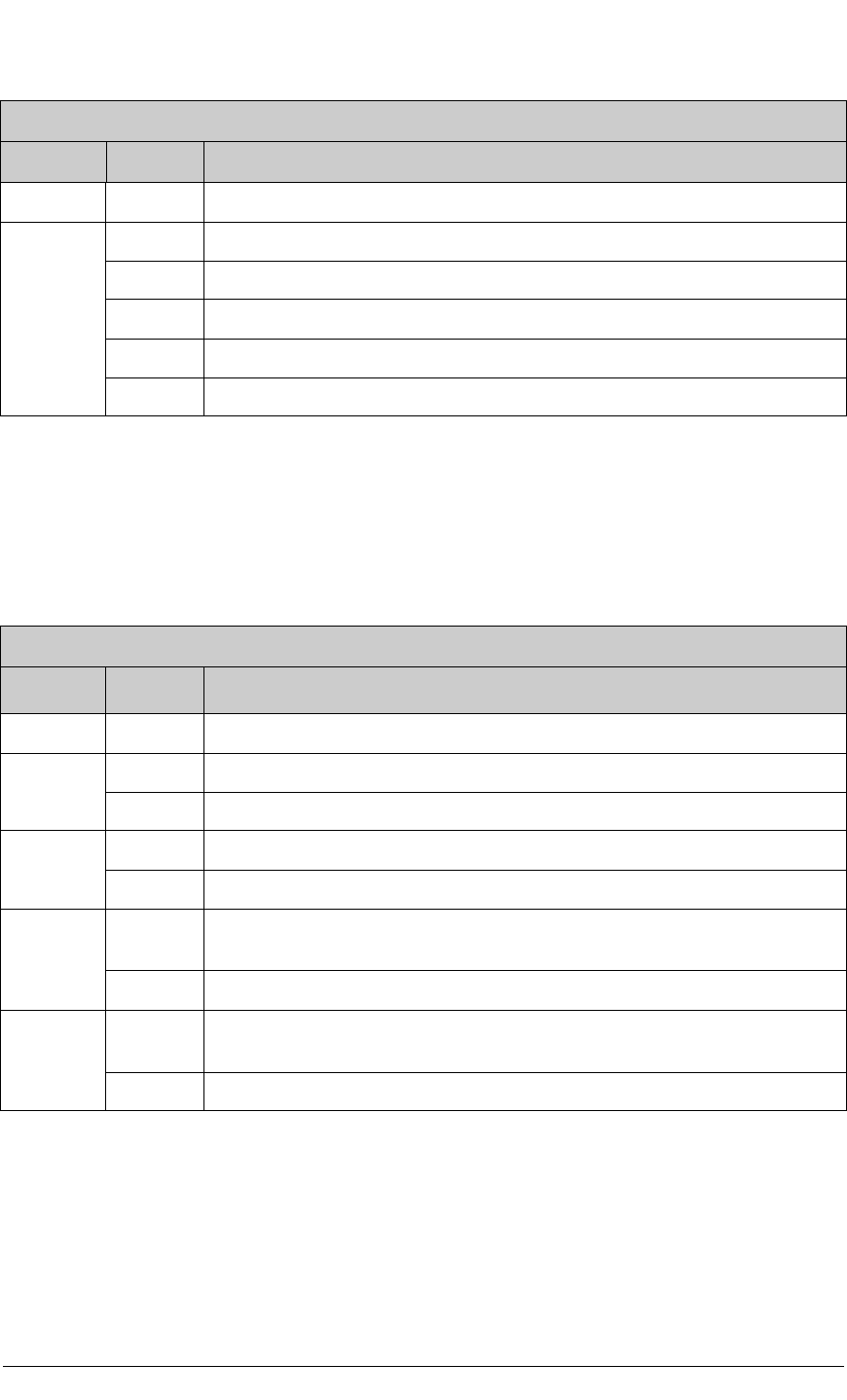
Table 8-5. MMU Expanded Code Register (MECR = 0x018)
MMU Expanded Code Register (MECR) (Address = 0x018)
Bit(s) Value Description
7:3 These bits are ignored for write, and return zeros when read.
2:0
0xx Normal operation.
100 For an XPC access, use MB0CR independent of A19-A18.
101 For an XPC access, use MB1CR independent of A19-A18.
110 For an XPC access, use MB2CR independent of A19-A18.
111 For an XPC access, use MB3CR independent of A19-A18.
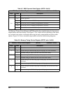
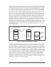
Table 8-6. Memory Timing Control Register (MTCR, adr = 0x019)
Memory Timing Control Register (MTCR) (Address = 0x019)
Bit(s) Value Description
7:4 xxxx These bits are reserved and should not be used.
3 0 Normal timing for /OE1B (rising edge to rising edge, one clock minimum).
1 Extended timing for /OE1B (one-half clock earlier than normal).
2 0 Normal timing for /OE0B (rising edge to rising edge, one clock minimum).
1 Extended timing for /OE0B (one-half clock earlier than normal).
10
Normal timing for /WE1B (rising edge to falling edge, one and one-half clocks
minimum).
1 Extended timing for /WE1B (falling edge to falling edge, two clocks minimum).
00
Normal timing for /WE0B (rising edge to falling edge, one and one-half clocks
minimum).
1 Extended timing for /WE0B (falling edge to falling edge, two clocks minimum).