


User’s Manual 25
the root segment or it may contain data variables. The stack segment is normally 4K long
and it holds the system stack. The XPC segment is normally used to execute code that is
not stored in the root segment or the data segment. Special instructions support executing
code that is visible in the XPC segment.
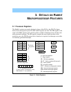
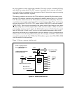
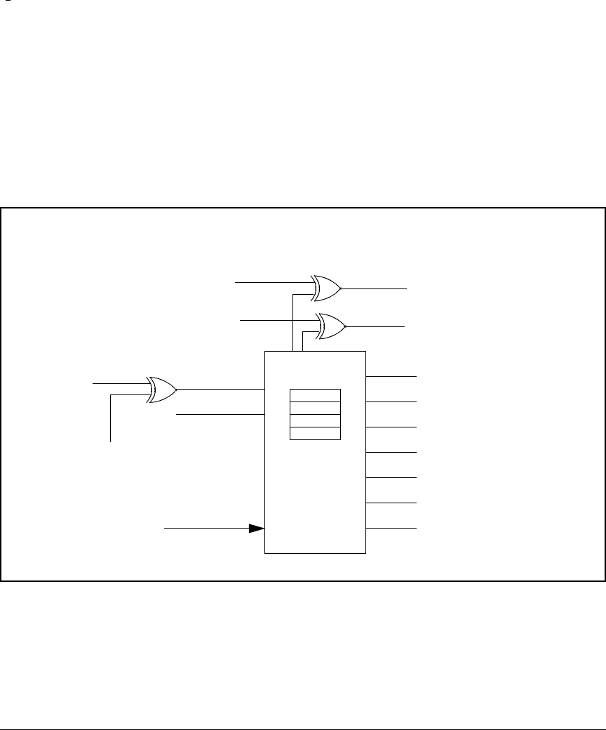
The memory interface unit receives the 20-bit addresses generated by the memory-map-
ping unit. The memory interface unit conditionally modifies address lines A16, A18 and
A19. The other address lines of the 20-bit address are passed unconditionally. The mem-
ory interface unit provides control signals for external memory chips. These interface sig-
nals are chip selects (/CS0, /CS1, /CS2), output enables (/OE0, /OE1), and write enables
(/
WE0, /WE1). These signals correspond to the normal control lines found on static mem-
ory chips (chip select or /CS, output enable or /OE, and write enable or /WE). In order to
generate these memory control signals, the 20-bit address space is divided into four quad-
rants of 256K each. A bank control register for each quadrant determines which of the
chip selects and which pair of output enables, and write enables (if any) is enabled when a
memory read or write to that quadrant takes place. For example, if a 512K x 8 flash mem-
ory is to be accessed in the first 512K of the 20-bit address space, then /CS0, /WE0, /OE0
could be enabled in both quadrants.
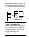
Figure 3-4 shows a memory interface unit.
Figure 3-4. Memory Interface Unit
/CS0
/CS1
/CS2
/OE0
/WE0
/OE1
/WE1
A19in
A18in
A18
A19
A18in
A19in
A19in'
Optional A19 inversion
memory
control
memory
control
lines
A18, A19 invertible
by quadrant
Read/Write
Synchronization
Axxin—from processor
Axx—out from memory
control unit
Address lines not shown
are passed directly.