


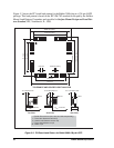
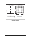
62 Rabbit 3000 Microprocessor
5.3 Rabbit Pin Descriptions
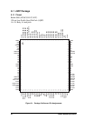
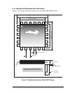
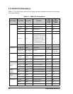
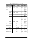
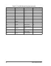
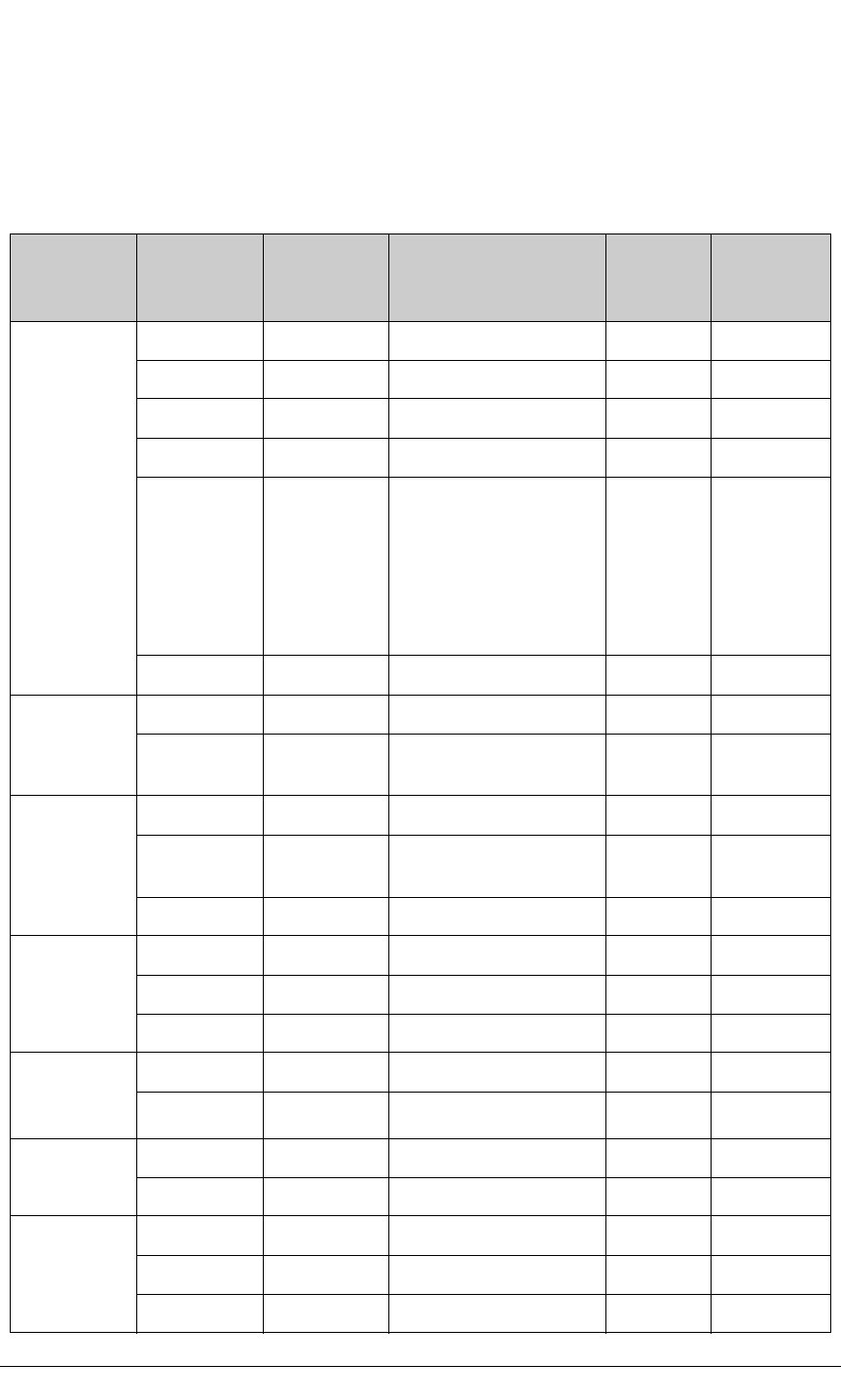
Table 5-1 lists all the pins on the device, along with their direction, function, and pin num-
ber on the package.
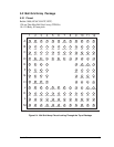
Table 5-1. Rabbit Pin Descriptions
Pin Group Pin Name Direction Function
Pin
Numbers
LQFP
Pin
Numbers
TFBGA
Hardware CLK Output Internal Clock 2 B1
CLK32K Input 32 kHz Oscillator In 49 L6
/RESET Input Master Reset 46 M5
RESOUT Output Reset Output 50 M6
XTALA1 Input
Main Oscillator In—if an
external clock is used, this
pin should be driven by
the external clock; see
Technical Note TN235 for
more information on
external oscillator circuits
113 B7
XTALA2 Output Main Oscillator Out 114 A7
CPU Buses ADDR[19:0] Output Address Bus various
DATA[7:0] Bidirectional Data Bus
10–15, 18–
19
D4, E1–E4,
F1, F4, G0
Status/Control /WDTOUT Output WDT Time-Out 43 J5
STATUS Output
Instruction Fetch First
Byte
4C1
SMODE[1:0] Input Bootstrap Mode Select 44, 45 K5, L5
Memory Chip
Selects
/CS0 Output Memory Chip Select 0 7 D1
/CS1 Output Memory Chip Select 1 47 J6
/CS2 Output Memory Chip Select 2 3 B2
Memory
Output
Enables
/OE0 Output Memory Output Enable 0 5 C2
/OE1 Output Memory Output Enable 1 95 C12
Memory
Write Enables
/WE0 Output Memory Write Enable 0 86 F9
/WE1 Output Memory Write Enable 1 99 B11
I/O Control /BUFEN Output I/O Buffer Enable 42 M4
/IORD Output I/O Read Enable 41 L4
/IOWR Output I/O Write Enable 40 K4