


User’s Manual 67
The alternate output functions identified in Table 5-2 are configured by setting the appro-
priate bits in the Paralle Port x Function Register.
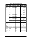
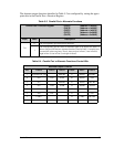
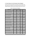
Table 5-3. Parallel Port x Alternate Functions
Parallel Port x Function Register (PCFR) (Address = 0x0055)
(PDFR) (Address = 0x0065)
(PEFR) (Address = 0x0075)
(PFFR) (Address = 0x003D)
(PGFR) (Address = 0x004D)
Bit(s) Value Description
7:0
0 The corresponding port bit functions normally.
1
The corresponding port bit carries its alternate signal as an output. See Table 5-4
below. Only the bits that have alternate functions listed in Table 5-4 actually have
a control bit in these registers. That is, there are four in Port C, four in Port D,
eight in Port E, four in Port F, and eight in Port G.
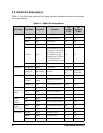
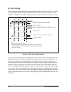
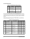
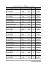
Table 5-4. Parallel Port x Alternate Functions Control Bits
Alternate Output Function
Bit Port B Port C Port D Port E Port F Port G
7 /SLAVEATTN, IA5 APWM3 I7 PWM3 APWM1
6 IA4 TXA ATXA I6 PWM2 TXE
5 IA3 APWM2 I5 PWM1 RCLKE
4 IA2 TXB ATXB I4 PWM0 TCLKE
3 IA1 I3 APWM0
2 IA0 TXC I2 TXF
1 CLKA I1 CLKC RCLKF
0 CLKB TXD I0 CLKD TCLKF