


User’s Manual 143
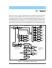
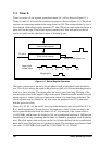
9.7 Parallel Port G
Parallel Port G is a byte-wide port with each bit programmable for data direction and
drive. These are simple inputs and outputs controlled and reported in the Port G Data Reg-
ister. As outputs, the bits of the port are buffered, with the data written to the Port G Data
Register transferred to the output pins on a selected timing edge. The outputs of Timer A1,
Timer B1, or Timer B2 can be used for this function, with each nibble of the port having a
separate select field to control this timing.
These inputs and outputs are also used for access to other peripherals on the chip. As out-
puts, Port G can carry the data and clock outputs from Serial Ports E and F. As inputs, Port
G can carry the data and clock inputs for these two serial ports.
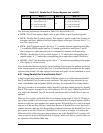
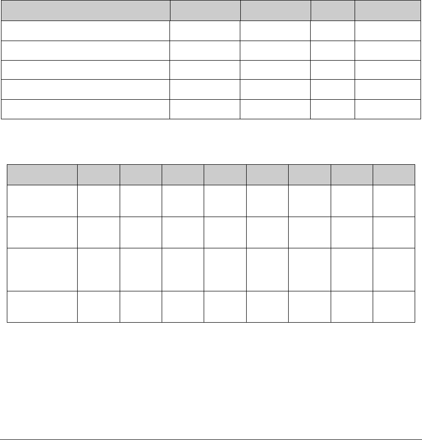
The following registers are described in Table 9-17 and in Table 9-18.
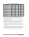
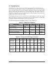
Table 9-16. Parallel Port G Registers
Register Name Mnemonic I/O address R/W Reset
Port G Data Register PGDR 0x48 R/W xxxxxxxx
Port G Control Register PGCR 0x4C W xx00xx00
Port G Function Register PGFR 0x4D W xxxxxxxx
Port G Drive Control Register PGDCR 0x4E W xxxxxxxx
Port G Data Direction Register PGDDR 0x4F W 00000000
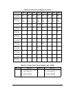
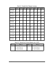
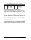
Table 9-17. Parallel Port G Data Register Functions
Bit 7 Bit 6 Bit 5 Bit 4 Bit 3 Bit 2 Bit 1 Bit 0
PGDR (R/W)
adr = 0x048
PG7 PG6 PG5 PG4 PG3 PG2 PG1 PG0
PGFR (W)
adr = 0x04D
x
SOUT_E RCLK_E TCLK_E x SOUT_F RCLK_F TCLK_F
PGDCR (W)
adr = 0x04E
out =
open
drain
out =
open
drain
out =
open
drain
out =
open
drain
out =
open
drain
out =
open
drain
out =
open
drain
out =
open
drain
PGDDR (W)
adr = 0x04F
dir =
out
dir =
out
dir =
out
dir =
out
dir =
out
dir =
out
dir =
out
dir =
out