


User’s Manual 133
9.4 Parallel Port D
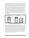
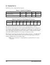
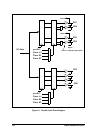
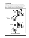
Parallel Port D, shown in Figure 9-1, has eight pins that can be programmed individually
to be inputs or outputs. When programmed as outputs, the pins can be individually
selected to be open-drain outputs or standard outputs. Port D pins can be addressed by bit
if desired. The output registers are cascaded and timer-controlled, making it possible to
generate precise timing pulses. Port D bits 4 and 5 can be used as alternate bits for Serial
Port B, and bits 6 and 7 can be used as alternate bits for Serial Port A. Alternate serial port
bit assignments make it possible for the same serial port to connect to different communi-
cations lines that are not operating at the same time.
On reset, the data direction register is zeroed, making all pins inputs. In addition certain
bits in the control register are zeroed (bits 0,1,4,5) to ensure that data is clocked into the
output registers when loaded. All other registers associated with port D are not initialized
on reset.
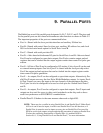
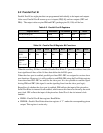
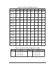
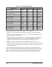
Table 9-7. Parallel Port D Registers
Register Name Mnemonic I/O address R/W Reset
Port D Data Register PDDR 0x60 R/W xxxxxxxx
Port D Control Register PDCR 0x64 W xx00xx00
Port D Function Register PDFR 0x65 W xxxxxxxx
Port D Drive Control Register PDDCR 0x66 W xxxxxxxx
Port D Data Direction Register PDDDR 0x67 W 00000000
Port D Bit 0 Register PDB0R 0x68 W xxxxxxxx
Port D Bit 1 Register PDB1R 0x69 W xxxxxxxx
Port D Bit 2 Register PDB2R 0x6A W xxxxxxxx
Port D Bit 3 Register PDB3R 0x6B W xxxxxxxx
Port D Bit 4 Register PDB4R 0x6C W xxxxxxxx
Port D Bit 5 Register PDB5R 0x6D W xxxxxxxx
Port D Bit 6 Register PDB6R 0x6E W xxxxxxxx
Port D Bit 7 Register PDB7R 0x6F W xxxxxxxx