


User’s Manual 83
7.3 Clock Doubler
The clock doubler is provided to allow a lower frequency crystal to be used for the main
oscillator and to provide an added range of clock frequency adjustability. The clock dou-
bler is controlled via the Global Clock Double Register as shown in Table 7-7.
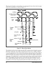
The clock doubler uses an on-chip delay circuit that must be programmed by the user at
startup if there is a need to double the clock. Table 7-8 lists the recommended delays for
the Global Clock Double Register for various oscillator frequencies.
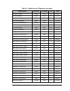
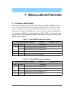
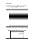
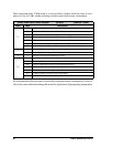
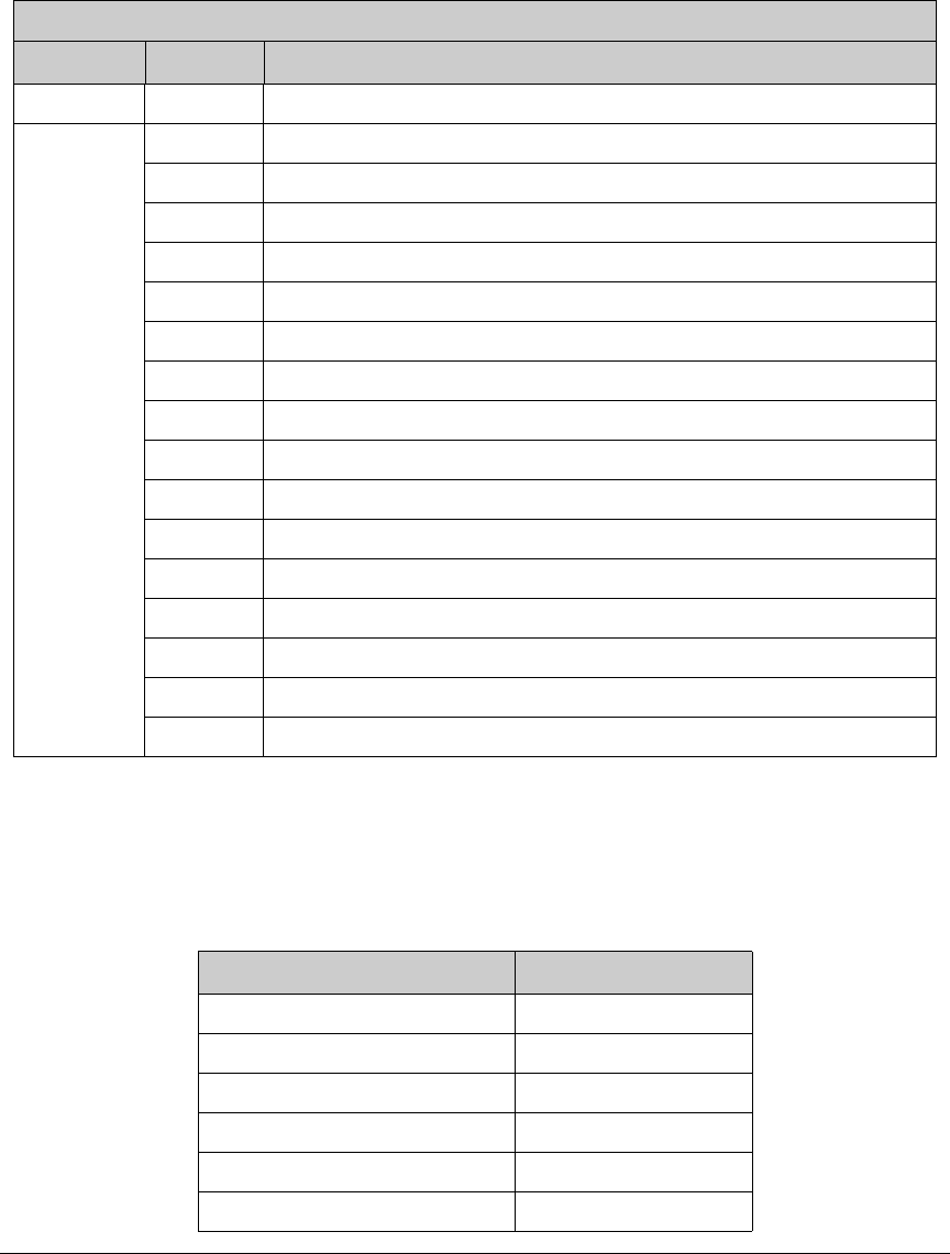
Table 7-7. Global Clock Double Register
Global Clock Double Register (GCDR) (Address = 0x0F)
Bit(s) Value Description
7:4 xxxx Reserved
3:0
0000 The clock doubler circuit is disabled.
0001 6 ns nominal low time
0010 7 ns nominal low time
0011 8 ns nominal low time
0100 9 ns nominal low time
0101 10 ns nominal low time
0110 11 ns nominal low time
0111 12 ns nominal low time
1000 13 ns nominal low time
1001 14 ns nominal low time
1010 15 ns nominal low time
1011 16 ns nominal low time
1100 17 ns nominal low time
1101 18 ns nominal low time
1110 19 ns nominal low time.
1111 20 ns nominal low time
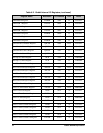
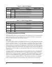
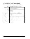
Table 7-8. Recommended Delays Set In GCDR for Clock Doubler
Recommended GCDR Value Frequency Range
15 ≤7.3728 MHz
13 7.3728–11.0592 MHz
9 11.0592–16.5888 MHz
6 16.5888–20.2752 MHz
3 20.2752–52.8384 MHz
0 >52.8384 MHz