


218 Rabbit 3000 Microprocessor
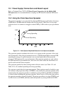
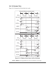
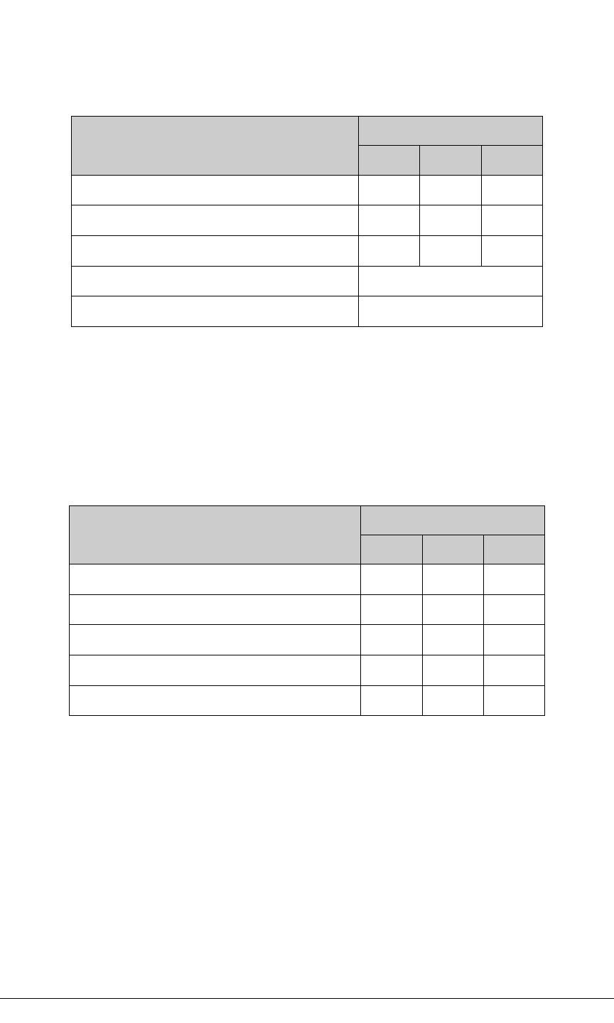
The following memory read time delays were measured.
The measurements were taken at the 50% points under the following conditions.
• T = -40°C to 85°C, V = 3.3 V
• Internal clock to nonloaded CLK pin delay ≤ 1 ns @ 85°C/3.0 V
The following memory write time delays were measured.
The measurements were taken at the 50% points under the same conditions that the mem-
ory read delays were measured.
See Table 16-2 for delays at other voltages.
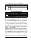
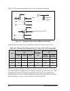
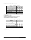
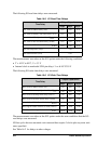
Table 16-3. Memory Read Time Delays
Time Delay
Output Capacitance
30 pF 60 pF 90 pF
Max. clock to address delay (T
adr
)
6 ns 8 ns 11 ns
Max. clock to memory chip select delay (T
CSx
)
6 ns 8 ns 11 ns
Max. clock to memory read strobe delay (T
OEx
)
6 ns 8 ns 11 ns
Min. data setup time (T
setup
)
1 ns
Min. data hold time (T
hold
)
0 ns
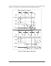
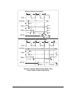
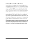
Table 16-4. Memory Write Time Delays
Time Delay
Output Capacitance
30 pF 60 pF 90 pF
Max. clock to address delay (T
adr
)
6 ns 8 ns 11 ns
Max. clock to memory chip select delay (T
CSx
)
6 ns 8 ns 11 ns
Max. clock to memory write strobe delay (T
WEx
)
6 ns 8 ns 11 ns
Max. high Z to data valid rel. to clock (T
DHZV
)
10 ns 12 ns 15 ns
Max. data valid to high Z rel. to clock (T
DVHZ
)
10 ns 12 ns 15 ns