


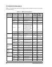
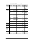
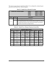


User’s Manual 63
I/O ports PA[7:0] Input / Output I/O Port A 111–104
D7, A8, B8,
C8, D8, A9,
B9, C9
I/O ports
(continued) PB[7:0] Input / Output I/O Port B 123–116
C4, A5, B5,
C5, D5, A6,
B6, C6
PC[7:0] 4 In / 4 Out I/O Port C
66–71, 74,
75
L11, M11,
M12, L12,
K12, K11,
J10, H12
PD[7:0] Input / Output I/O Port D 52–59
K7, L7, M7,
J8, K8, L8,
M8, J9
PE[7:0] Input / Output I/O Port E
26–31, 34,
35
H4, J1–J4,
K1, L1–L2
PF[7:0] Input / Output I/O Port F
127–124,
103–100
A3, B3, A4,
B4, A10,
B10, A11,
A12
PG[7:0] Input / Output I/O Port G
36–38, 60–
63
M1, M2, L3,
M3, K9, L9,
M9, K10
Power,
processor core
VDDCORE +3.3 V
8, 24, 72,
88
D2, E11, H2,
J12
Power
Processor I/O
Ring
VDDIO +3.3 V
1, 17, 33,
65, 81, 97,
115
A1, C10, D6,
F3, G10, K3,
M10
Power Battery
Backup
VBAT +3.3 V or battery 51 J7
Ground
Processor
Core
VSSCORE Ground
9, 25, 73,
89
D3, E10, H3,
J11
Ground
Processor I/O
Ring
VSSIO Ground
16, 32, 48,
64, 80, 96,
112, 128
A2, C7, C11,
F2, G11, K2,
K6, L10
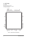
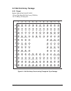
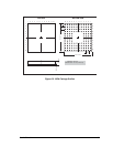
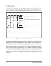
Table 5-1. Rabbit Pin Descriptions (continued)
Pin Group Pin Name Direction Function
Pin
Numbers
LQFP
Pin
Numbers
TFBGA