


User’s Manual 305
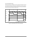
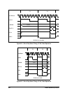
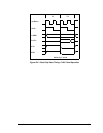
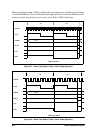
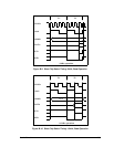
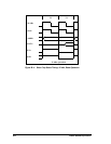
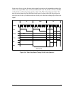
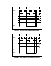
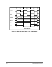
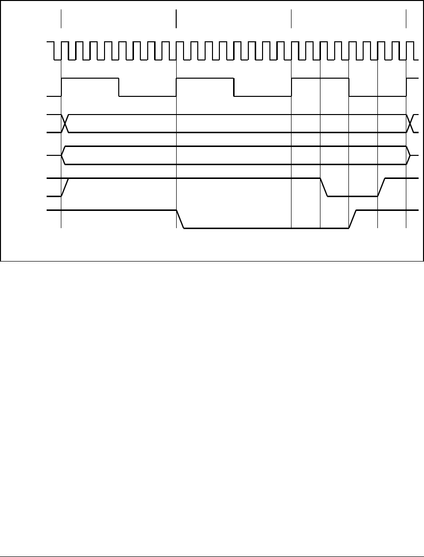
In the case of write cycles, the chip select signals are active only around the trailing edge
of the write signal. Wait states are inserted between T1 and T2, and this will have no effect
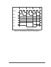
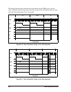
on the duration of the chip select signals in this mode. The timing diagrams below illus-
trate the actual timing for the different divided cases. In these cases the chip selects are
active for two clock cycles before and two clock cycles after the trailing edge of the write
signal.
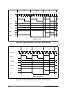
Figure B-12. Short Chip Select Timing: CLK/8, Write Operation
oscillator
ADDR
DATA
T1 TWA
Val id
/WEx
/CSx
clock
divi de-b
y
-8 mod
e
T2