


User’s Manual 201
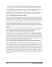
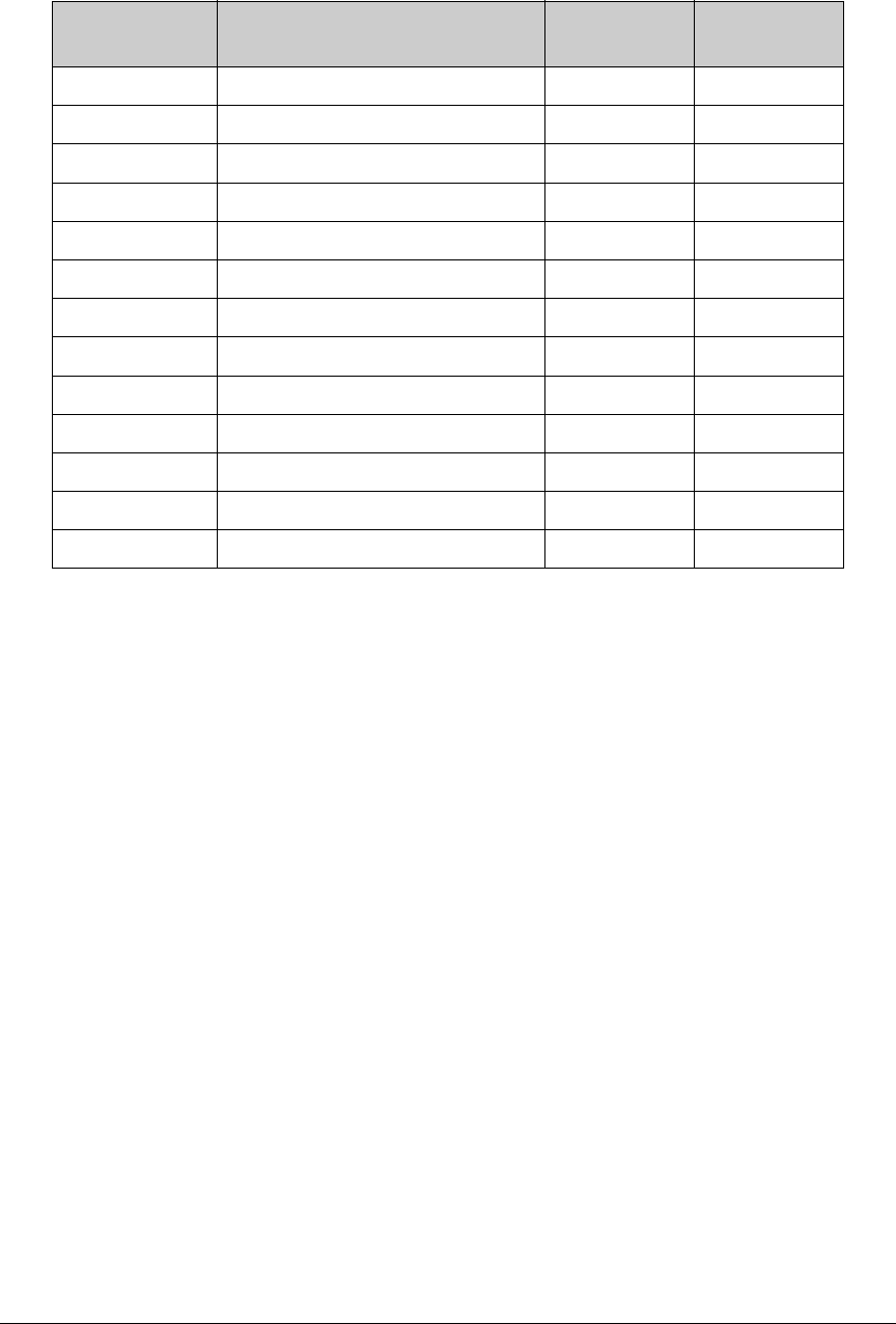
The following table explains the parameters used in Figure 13-2.
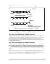
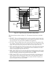
The two SPD0R registers have special functionality not shared by the other data registers.
If the master writes to SPD0R, an inbound interrupt flip-flop is set. If slave port interrupts
are enabled, the slave processor will take a slave port interrupt. If the slave writes to the
other SPD0R register, the slave attention line (/SLAVEATTN, pin 100) is asserted (driven
low) by the slave processor. This line can be used to create an interrupt in the master.
Either side that is interrupted can clear the signal that is causing an interrupt request by writ-
ing to the slave port status register. The data bits are ignored, but the flip-flop that is the
source of the interrupt request is cleared. Figure 13-3 shows a logical schematic of this func-
tionality.
Symbol Parameter
Minimum
(ns)
Maximum
(ns)
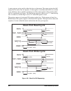
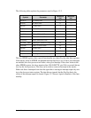
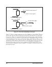
Tsu(SCS) /SCS Setup Time 5 —
Th(SCS) /SCS Hold Time 0 —
Tsu(SA) SA Setup Time 5 —
Th(SA) SA Hold Time 0 —
Tw(SRD) /SRD Low Pulse Width 40 —
Ten(SRD) /SRD to SD Enable Time 0 —
Ta(SRD) /SRD to SD Access Time — 30
Tdis(SRD) /SRD to SD Disable Time — 15
Tsu(SRW – SRD) /SWR High to /SRD Low Setup Time 40 —
Tw(SWR) /SWR Low Pulse Width 40 —
Tsu(SD) SD Setup Time 10 —
Th(SD) SD Hold Time 5 —
Tsu(SRD – SWR) /SRD High to /SWR Low Setup Time 40 —