


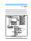
User’s Manual 157
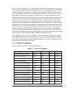
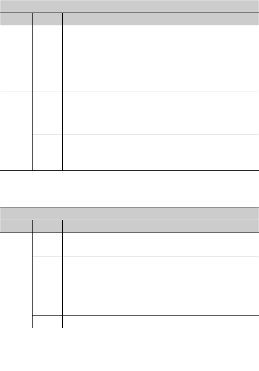
The control/status register for Timer B (TBCSR) is laid out as shown in Table 11-7.
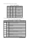
The control register for Timer B (TBCR) is laid out as shown in Table 11-8.
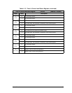
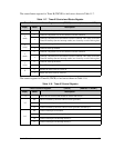
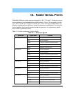
Table 11-7. Timer B Control and Status Register
Timer B Control and Status Register (TBCSR) (Address = 0x00B0)
Bit(s) Value Description
7:3 These bits are always read as zero.
2
(read)
0 Timer B2 comparator has not encountered a match condition.
1
Timer B2 comparator has encountered a match condition. This status bit and the
Timer B2 interrupt (but not interrupt enable) are cleared by a read of this register.
2
(write)
0 Timer B2 interrupt disabled.
1 Timer B2 interrupt enabled.
1
(read)
0 Timer B1 comparator has not encountered a match condition.
1
Timer B1 comparator has encountered a match condition. This status bit and the
Timer B1 interrupt (but not interrupt enable) are cleared by a read of this register.
1
(write)
0 Timer B1 interrupt disabled.
1 Timer B1 interrupt enabled.
0
0 Disable the main clock for Timer B.
1 Enable the main clock for Timer B.
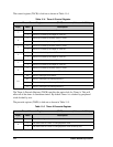
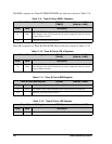
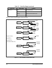
Table 11-8. Timer B Control Register
Timer B Control Register (TBCR) (Address = 0x00B1)
Bit(s) Value Description
7:4 These bits are reserved and should be written with zeroes.
3:2
00 Timer B clocked by the main Timer B clock (perclk/2).
01 Timer B clocked by the output of Timer A1.
1x Timer B clocked by the main Timer B clock (perclk/2) divided by 8.
1:0
00 Timer B interrupts are disabled.
01 Timer B interrupts use Interrupt Priority 1.
10 Timer B interrupts use Interrupt Priority 2.
11 Timer B interrupts use Interrupt Priority 3.