


216 Rabbit 3000 Microprocessor
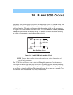
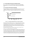
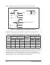
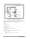
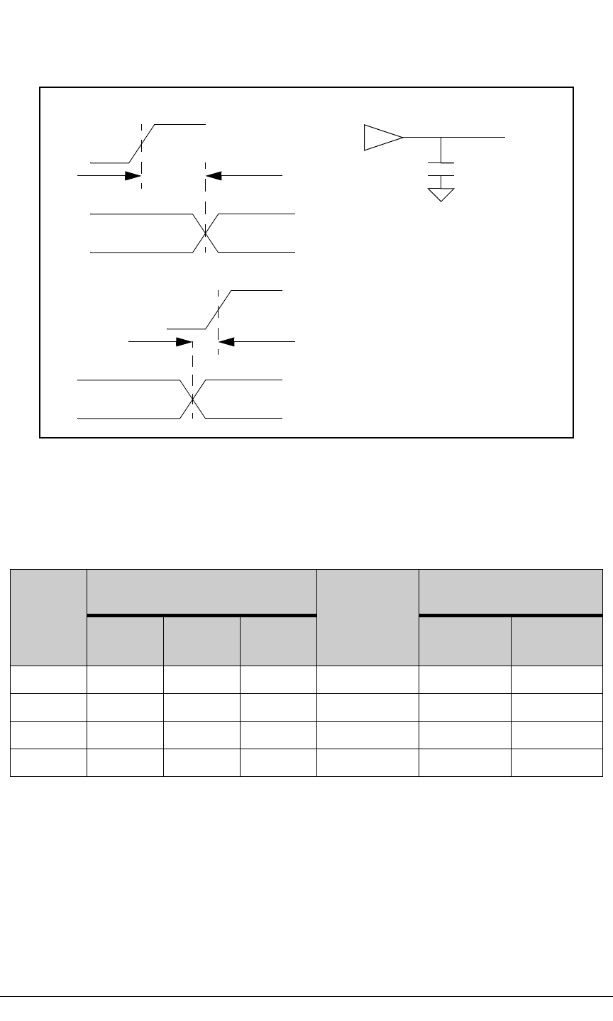
Figure 16-1 illustrates the parameters used to describe memory access time.
Figure 16-1. Parameters Used to Describe Memory Access Time
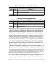
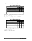
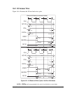
Table 16-2 lists the delays in gross memory access time for several values of V
DD
.
When the spectrum spreader is enabled with the clock doubler, every other clock cycle is
shortened (sometimes lengthened) by a maximum amount given in the table above. The
shortening takes place by shortening the high part of the clock. If the doubler is not
enabled, then every clock is shortened during the low part of the clock period. The maxi-
mum shortening for a pair of clocks combined is shown in the table.
Table 16-2. Data and Clock Delays V
DD
±10%, Temp, -40°C–+85°C (maximum)
VDD
Clock to Address Output Delay
(ns)
Data Setup
Time Delay
(ns)
Spectrum Spreader Delay
(ns)
30 pF 60 pF 90 pF
Normal
no dbl/dbl
Strong
no dbl/dbl
3.3 6 8 11 1 3/4.5 4.5/9
2.7 7 10 13 1.5 3.5/5.5 5.5/11
2.5 8 11 15 1.5 4/6 6/12
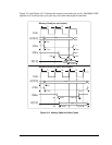
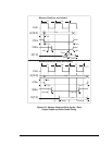
1.8 18 24 33 3 8/12 11/22
delay capacitive
loading
setup time data to clock