


User’s Manual 221
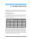
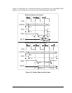
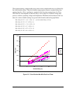
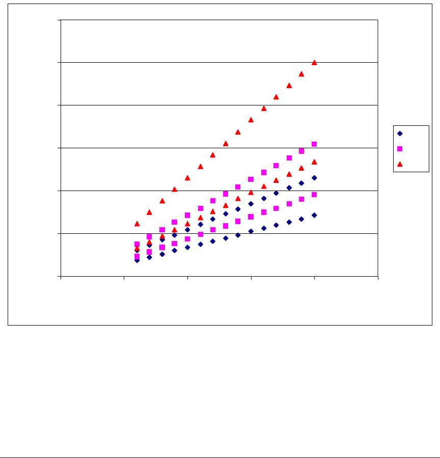
The required memory output enable access time is more complicated since it is affected by
the clock doubler delays. The clock doubler setup register creates a nominal delay time
ranging from 6 to 20 ns, resulting in a nominal clock low time ranging from 6 to 20 ns.
The clock low time depends on internal delays, and is subject to variation arising from
process variation, operating voltage and temperature. Minimum and maximum clock low
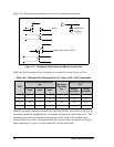
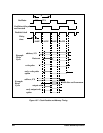
times for various doubler settings are given in the formulas and in the graph below.
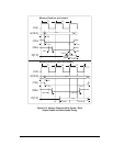
Max. delay @ 3.3 V = 6.1 + 1.21(n - 6) [n is the nominal delay, 6–20 ns)
Min. delay @ 3.3 V = 3.7 + 0.75(n - 6)
Max. delay @ 2.5 V = 7.6 + 1.67(n - 6)
Min. delay @ 2.5 V = 4.7 + 1.03(n - 6)
Max. delay @ 1.8 V = 12.2 + 2.7(n - 6)
Min. delay @ 1.8 V = 6.6 + 1.44(n - 6)
Figure 16-5. Clock Doubler Max-Min Clock Low Times
0.0
10.0
20.0
30.0
40.0
50.0
60.0
0 5 10 15 20 25
Nominal Delay (ns)
Delay (ns)
3.3 V
2.5 V
1.8 V