Instruction Syntax and Addressing Modes
4-16
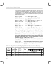
Example 4.3.12 MOV *R5++R5, A0~, ++A
Refer to the initial processor state in Table 4–8 before execution of this
instruction. Preincrement AP0. After preincrement, A0 is AC3 and A0~ is
AC19. The contents of AC19 are stored in the data memory location in R5. R5
is then incremented by R5. Final result, AP0=3, R5 = 0x0004, *0x0002 =
0xFEED.
Example 4.3.13 MOV A2, *R0
Refer to the initial processor state in Table 4–8 before execution of this instruc-
tion. The contents of the data memory address in R0 are loaded into A2
(AC11). Final result, AC11 = 0x0400. Note the addressing is byte addressing.
Thus, *R0 = 0x0454 indicates the word memory location 0x454/2 = 0x022A.
Example 4.3.14 IN *R4++, 0x00
The contents of the I/O port location 0x00 (port PPA) are stored in the location
pointed to by R4. R4 is incremented by 2 after this operation.
Example 4.3.15 MOVB *R7++, A3
Refer to the initial processor state in Table 4–8 before execution of this instruc-
tion. Store the lower 8 bits of A3 (AC29) in the data memory byte address
pointed to by R7. R7 is then incremented by one. Notice that to find the word
address, divide the address in R7 by 2. Final result, R7=0x0101, *0x0100 =
0xAB (byte address) or *0x80 = 0xAB00 (word address).
Example 4.3.16 OUT 0x08, *R1––
Refer to the initial processor state in Table 4–8 before execution of this instruc-
tion. The contents of the data memory byte location stored in R1 are placed
on port 0x08 (port PPB). R1 is then decremented by 2. Final result, R1 =
0x01FE, *0x08 = 0xCB. Port PPB is 8-bits wide, so the upper 8-bits of *R1
(0x0A) are ignored.
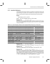
4.3.6 Relative Addressing
There are three types of relative addressing on the MSP50P614/MSP50C614:
short relative, long relative, and relative to the index register, R5. These ad-
dressing modes are described below.
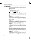
4.3.6.1 Relative to Index Register R5
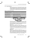
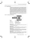
This relative addressing mode uses one of the 8 address registers (R0–R7)
as a base value. The index register, R5, is added to the base address value
in Rx. The base address register is not modified. Thus, the effective address
is Rx + R5.
Syntax:
name [dest,] [src,] *Rx+R5 [, next A]
name *Rx+R5 [, src] [, next A]


