


Input/Output Instructions
4-59Assembly Language Instructions
4.10 Input/Output Instructions
The MSP50P614/MSP50C614 processor communicates with other on-chip
logic as well as external hardware through a parallel I/O interface. Up to 40 I/O
ports are addressable with instructions that provide bidirectional data transfer
between the I/O ports and the accumulators.
Data input is performed with the IN instruction (Class 6). This instruction uses
a memory address and a 4-bit port address. It can also use an accumulator
(or offset accumulator) and a 6-bit port address. String transfers are allowed
between the accumulators and the input port.
Data output is performed with the OUT instruction (Class 6). The OUT
instruction can specify a memory address and a 4-bit port address. It can also
use an accumulator (or offset accumulator) and a 6-bit port address. String
transfers are allowed between the accumulators and the output port.
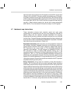
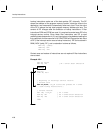
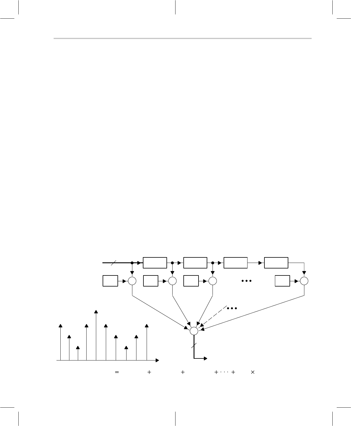
4.11 Special Filter Instructions
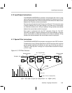
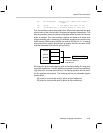
The MSP50P614/MSP50C614 processor can perform some DSP functions.
Fundamental to many filtering algorithms is the FIR structure which requires
several parallel operations to execute for each tap of the filter as shown in
Figure 4–5. Each tap has 1 multiply and 1 accumulation to obtain the output,
y, for N+1 taps,
Figure 4–5. FIR Filter Structure
Delay
16
Samples, x[k]
Newest sample
x[k]
x
h[0]
Delay
x[k–1]
x
h[1]
Delay
x[k–2]
x
h[2]
Delay
Oldest sample
x[k-N]
x
h[N]
+
32 or 48
N+1 Tap FIR filter
t
x[k–3]
x[k–2]
x[k–1]
x[k]
x[k+1]
x[k+2]
y[k] = Σ
m=0..N
h[m]⋅x[k-m]
y[k] h[0] x[k] h[1]x[k-1] h[2]x[k-2] h[N] x[k-N]