


Clock Control
2-29MSP50C6xx Architecture
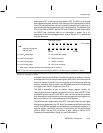
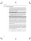
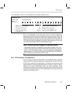
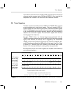
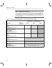
The configuration of bits in the clock speed control register appears below:
ClkSpdCtrl register
address 0x3D (16-bit wide location)
WRITE only 15 14 13 12 11 10 09 08 07 06 05 04 03 02 01 00
T5 T4 T3 T2 T1 I C or T0 R MMMMMMMM
T : RTO oscillator-Trim adjust R : enable Resistor-trimmed oscillator
I : Idle State clock Control M : PLLM multiplier bits for MC
C : enable Crystal oscillator
(or T0 if R is set
0x0000 : default state after RESET LOW
Bit 10 in the ClkSpdCtrl is idle state clock control. The level of deep-sleep
generated by the IDLE instruction is partially controlled by this bit. When this
bit is cleared (default setting), the CPU clock is stopped during the sleep, but
the MC remains running. When the idle state clock control bit is set, both the
CPU clock and the MC are stopped during sleep. Refer to section 2.11 for more
information regarding the C6xx’s reduced-power modes.
Note: Reference Oscillator Stopped by Programmed Disable
If the reference oscillator is stopped by a programmed disable, then, on re-
enable, the oscillator requires some time to restart and resume its correct fre-
quency. This time imposes a delay on the core processor resuming full-
speed operation. The time-delay required for the CRO to start is GREATER
than the time-delay required for the RTO to start.
2.8.4 RTO Oscillator Trim Adjustment
Bits 15 through 11 and bit 9 (6 bits total) in the ClkSpdCtrl effect a software
control for the RTO oscillator frequency. The purpose of this control is to trim
the RTO to its rated (32 kHz) specification. The correct trim value varies from
device to device. The user must program bits 15 through 11 and 9, in order to
achieve the 32-kHz specification within the rated tolerances. Texas
Instruments provides the trim value to the programmer of the P614 part with
a sticker on the body of the chip. For the C6xx parts, the correct trim value is
located at I/O location 0x2Fh.