


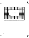
Mechanical Information
7-4
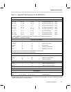
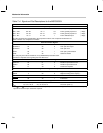
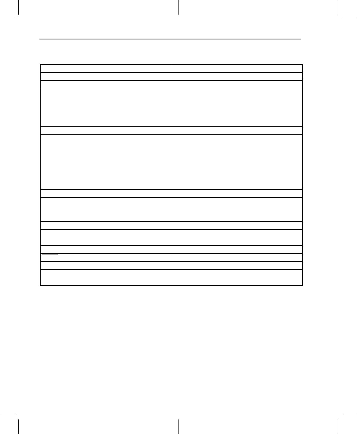
Table 7–2. Signal and Pad Descriptions for the MSP50C605
SIGNAL PIN NUMBER PAD NUMBER I/O DESCRIPTION
Input/Output Ports
PC0 – PC7 89 – 82 8 – 1 I/O Port C general-purpose I/O (1 Byte)
PD0 – PD7 99 – 92 18 – 11 I/O Port D general-purpose I/O (1 Byte)
PE0 – PE7 46 – 39 48 – 41 I/O Port E general-purpose I/O (1 Byte)
PF0 – PF7 16 – 9 31 – 24 I Port F dedicated input (1 Byte)
Pins PD
4
and PD
5
may be dedicated to the comparator function, if the comparator enable bit is set.
Refer to Section 3.3, Comparator, for details.
Scan Port Control Signals
SCANIN 37 39 I Scan port data input
SCANOUT 33 35 O Scan port data output
SCANCLK 36 38 I Scan port clock
SYNC 35 37 I Scan port synchronization
TEST 34 36 I C605: test modes
The scan port pins must be bonded out on any MSP50C605 production board.
Consult the “Important Note regarding Scan Port Bond Out”.
Reference Oscillator Signals
OSCOUT 49 51 O Resistor/crystal reference out
OSCIN 48 50 I Resistor/crystal reference in
PLL 47 49 O Phase-lock-loop filter
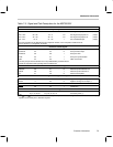
Digital-to-Analog Sound Outputs
DACP 7 22 O Digital-to-analog plus output (+)
DACM 5 20 O Digital-to-analog minus output (–)
Initialization
RESET 38 40 I Initialization
Power Signals
V
SS
17, 50, 90, 100
†
32, 52, 9, 19
†
Ground
V
DD
6
†
, 8, 31, 32, 91 21
†
, 23, 33, 34, 10 Processor power (+)
†
The V
SS
and V
DD
connections service the DAC circuitry. Their pins tend to sustain a higher current draw. A dedicated decoupling
capacitor across these pins is therefore required.