


Memory Organization: RAM and ROM
2-17MSP50C6xx Architecture
When writing to any of the locations in the I/O address map, therefore, the
bit-masking need only extend as far as width of location. Within a 16-bit
accumulator, the desired bits (width of location) should be right-justified. The
write operation is accomplished using the OUT instruction, with the address
of the I/O port as an argument.
A read from these locations is accomplished using the IN instruction, with the
address of the I/O port as an argument. When reading from the I/O port to a
16-bit accumulator, the IN instruction automatically clears any extra bits in
excess of width of location. The desired bits in the result will be right-justified
within the accumulator.
Allowable access indicates whether the port is bidirectional, read-only, or
write-only. The last column of the table points to the section in this manual
where the functions of each bit have been defined in more detail.
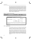
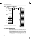
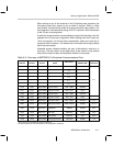
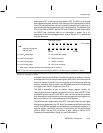
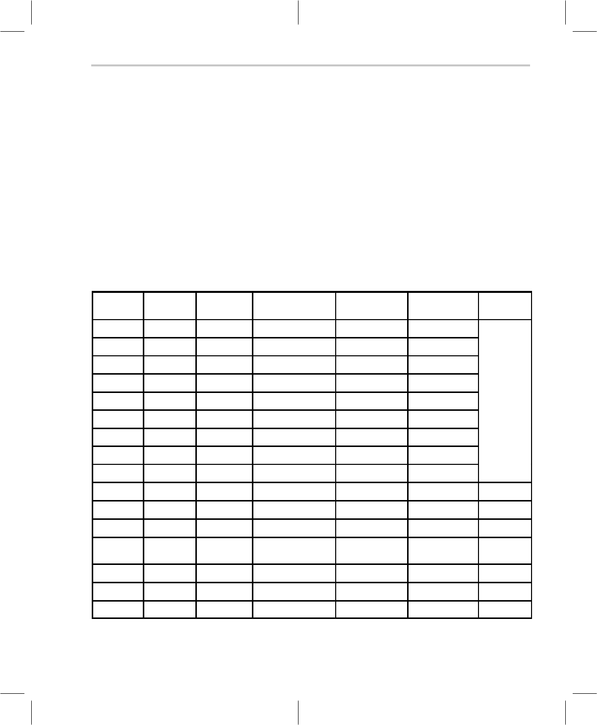
Table 2–2. Summary of MSP50C614’s Peripheral Communications Ports
I/O Map
Address
Width of
Location
Allowable
Access
Control Register
Name
Abbreviation
State after
RESET LOW
Section for
Reference
0x00 8 bits Read & Write I/O port A data PA
0..7
Data unknown†
0x04 8 bits Read & Write I/O port A control PA
0..7
Ctrl 0x00 ‡
0x08 8 bits Read & Write I/O port B data PB
0..7
Data unknown
0x0C 8 bits Read & Write I/O port B control PB
0..7
Ctrl 0x00
0x10 8 bits Read & Write I/O port C data PC
0..7
Data unknown
3.1.1
0x14 8 bits Read & Write I/O port C control PC
0..7
Ctrl 0x00
0x18 8 bits Read & Write I/O port D data PD
0..7
Data unknown
0x1C 8 bits Read & Write I/O port D control PD
0..7
Ctrl 0x00
0x20 8 bits Read & Write I/O port E data PE
0..7
Data unknown
0x24 8 bits Read & Write I/O port E control PE
0..7
Ctrl 0x00
0x28 8 bits Read Only Input port F data PF
0..7
Data unknown 3.1.2
0x2C 16 bits Read & Write Output port G data PG
0..15
Data 0x0000 3.1.3
0x2F 17 bits Read Only
RTO oscillator trim
adjustment
RTRIM 0x0000 2.8.4
0x30 16 bits Write Only DAC data DAC Data 0x0000 3.2.2
0x34 4 bits Read & Write DAC control DAC Ctrl 0x0 3.2.2
0x38 16 bits Read & Write Interrupt/general Ctrl IntGenCtrl 0x0000 3.4
†
Input states are provided by the external hardware.
‡
A control register value of 0x00 yields a port configuration of all inputs.