Clock Control
2-30
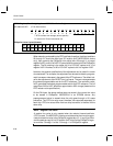
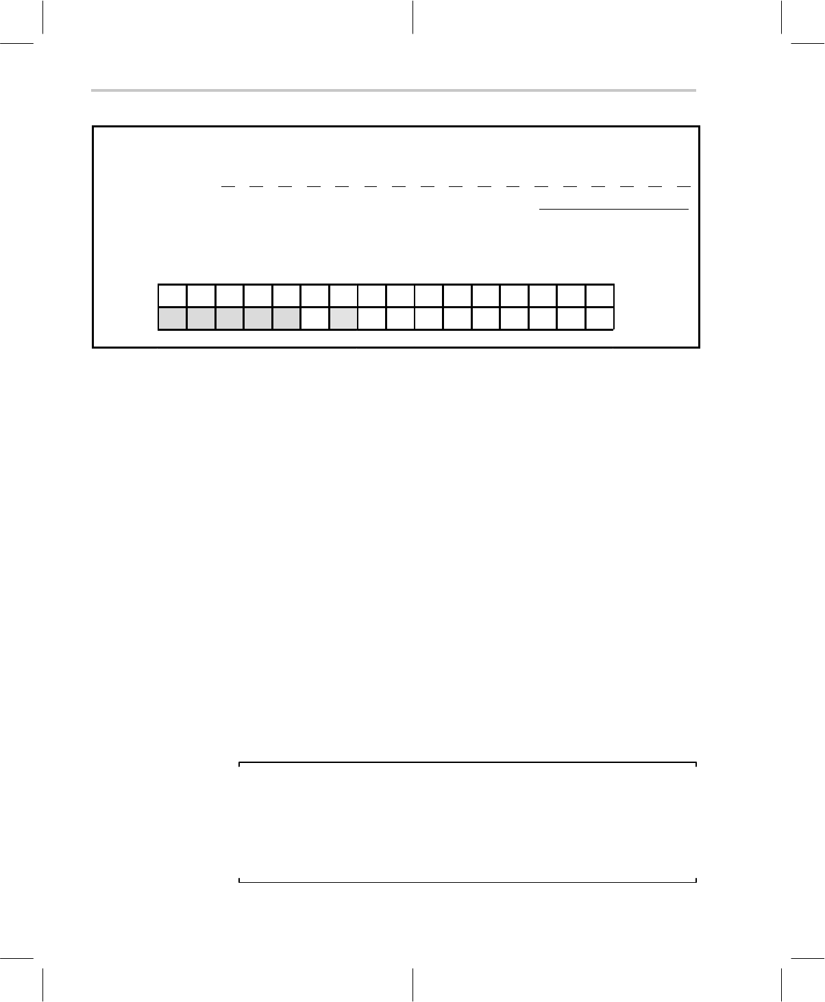
RTRIM Register (Read Only) (Applies to MSP50C6xx Device Only)
I/O Address 0x2Fh (17-bit wide location)
16 15 14 13 12 11 10 09 08 07 06 05 04 03 02 01 00
RRRRRRRRRRRT5T4T3T2T1T0
T: RTO oscillator-trim storage (device specific)
R: reserved for Texas Instruments use
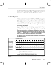
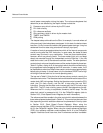
ClkSpdCtrl Value Copied (Shaded)
15 14 13 12 11 10 9 8 7 6 5 4 3 2 1 0
T5 T4 T3 T2 T1 I T0 1 M7 M6 M5 M4 M3 M2 M1 M0
When selecting and enabling the RTO oscillator,therefore, the bits at positions
05 through 01 should be read from I/O location 0x2F (MSP50C6xx device
only), then copied to the ClkSpdCtrl trim adjust (bits 15 through 11 of control
register 0x3D), and bit 0 of 0x2F I/O port should be copied to bit 9 of ClkSpdCtrl
register. The bit ordering is the same; bit 04 of I/O 0x2F copies to bit 15 of
register 0x3D. Likewise, bit 00 of I/O 0x2F copies to bit 9 of register 0x3D.
However, the general specification of the adjustment can be useful in certain
circumstances. For example, the adjustment can be used to obtain a program-
matic increase or decrease in the speed of the RTO reference. The default val-
ue for the adjustment, after RESET low, is all zeros. The zero value generates
the slowest programmable rate for the RTO reference. The maximum value,
0x3F, generates the fastest programmable rate for the RTO reference. The full
range from 0x00 to 0x3F, effects an approximate +62% change (based on the
RTO resistor value specification).
On the P614 part, the above method does not cause in the correct trim value
to be loaded in ClkSpdCtrl. MSP50P614 is an EPROM device. Any
preprogrammed value is erased when the chip goes through a UV erase
procedure. The RTO trim value must, therefore, be computed separately for
each chip. RTO trim values differ from one chip to another, is identical for the
same chip.
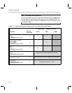
Note: Register Trim Value
A resistor trim value is only needed when the resistor trimmed oscillator
(RTO) is used. The MSP50P614 device must determine the trim value sepa-
rately and use this value in the ClkSpdCtrl register bits 15–11 and 9, but C6xx
device needs to copy bit 0 of I/O location 0x2F to bit 9 of the ClkSpdCtrl regis-
ter and bits 5 through 1 to bits 15 through 11 of ClkSpdCtrl register.


