


Memory Organization: RAM and ROM
2-18
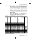
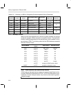
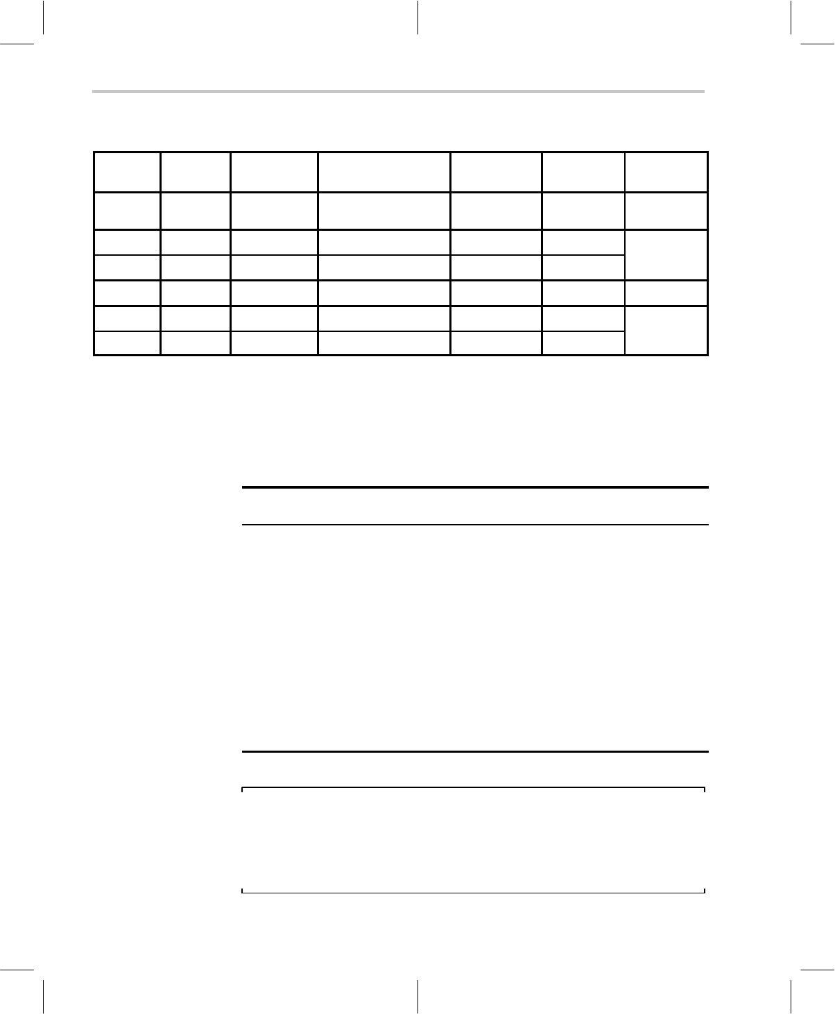
Table 2–2. Summary of C614’s Peripheral Communications Ports (Continued)
I/O Map
Address
Width of
Location
Allowable
Access
Control Register Name Abbreviation
State after
RESET LOW
Section for
Reference
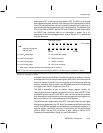
0x39 8 bits Read & Write Interrupt flag IFR
Same state as
before RESET
2.7
0x3A 16 bits Read & Write TIMER1 period PRD1 0x0000
28
0x3B 16 bits Read & Write TIMER1 count-down TIM1 0x0000
2
.
8
0x3D 16 bits Write Only Clock speed control ClkSpdCtrl 0x0000 2.9.3
0x3E 16 bits Read & Write TIMER2 period PRD2 0x0000
28
0x3F 16 bits Read & Write TIMER2 count-down TIM2 0x0000
2
.
8
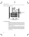
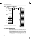
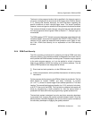
2.6.3 Interrupt Vectors
When its event has triggered and its service has been enabled, an interrupt
causes the program counter to branch to a specific location. The destination
location is stored (programmed) in the interrupt vector, which resides in an up-
per address of ROM. The following table lists the ROM address associated
with each interrupt vector:
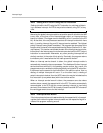
Interrupt Name
ROM address of
Vector
Event Source Interrupt Priority
INT0 0x7FF0 DAC Timer Highest
INT1 0x7FF1 TIMER1 2nd
INT2 0x7FF2 TIMER2 3rd
INT3 0x7FF3 port D
2
4th
INT4 0x7FF4 port D
3
5th
INT5 0x7FF5 all port F 6th
INT6 0x7FF6 port D
4
7th
INT7 0x7FF7 port D
5
Lowest
0x7FFE storage for ROM Protection Word
RESET
0x7FFF storage for initialization vector
Note: ROM Locations that Hold Interrupt Vectors
ROM locations that hold interrupt vectors are reserved specifically for this
purpose. Additional ROM locations 0x7FF8 - 0x7FFD are reserved for future
expansion. Like the interrupt vectors, they should not be used for general
program storage.