


I/O
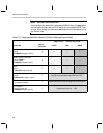
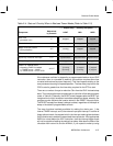
3-3Peripheral Functions
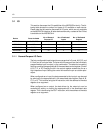
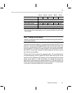
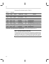
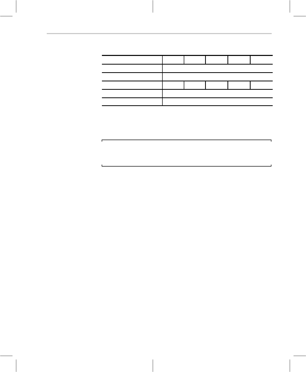
Port A Port B Port C Port D Port E
Control register address
0x04h
†
0x0Ch 0x14h 0x1Ch 0x24h
Possible control values 0 = High-Z INPUT 1 = TOTEM-POLE OUTPUT
Value after RESET low 0 = High-Z INPUT
Data register address 0x00h 0x08h 0x10h 0x18h 0x20h
Possible input data values Low = 0 High = 1 (don’t care on write)
Possible output data values 0 = Low 1 = High
†
Each of these I/O ports is only 8 bits wide. The reason for the 4-byte address spacing is so that
instructions
with limited addressability (such as memory transfers) can still access
these registers.
Note: Reading the Data Register
Whether configured as input or as output, reading the data register reads the
actual state of the pin.
The state of the control registers is initialized to 0x00 when the RESET pin is
taken low. This puts all of the programmable I/O pins into an input state. This
condition is maintained after RESET is taken high, and until the control regis-
ters are modified. The state of the data registers is not initialized with RESET.
After RESET is taken high, the state of the data registers is unknown and must
be initialized using software.
The 8-bit width is the true size of the mapped location. This is independent of
the address spacing, which is greater than 8-bits. When writing to any of the
locations in the I/O address map, therefore, the bit-masking need only extend
across 8 bits. Within a 16-bit accumulator, the desired bits should be
right-justified. When reading from these locations to a 16-bit accumulator, the
IN instruction automatically clears the extra bits in excess of 8. The desired bits
in the result will be right-justified within the accumulator.