


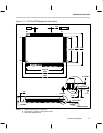
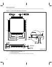
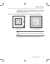
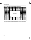
Mechanical Information
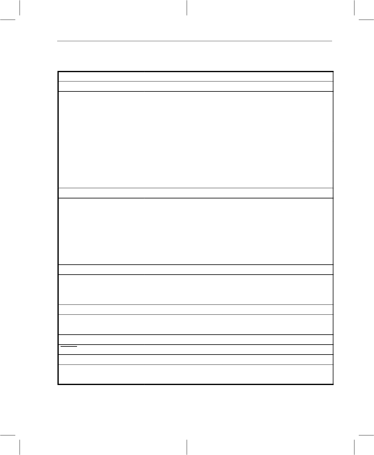
7-3Customer Information
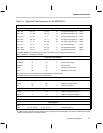
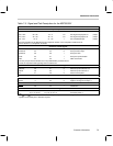
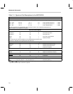
Table 7–1. Signal and Pad Descriptions for the MSP50C614
SIGNAL PIN NUMBER PAD NUMBER I/O DESCRIPTION
Input/Output Ports
PA0 – PA7 66 – 59 75 – 68 I/O Port A general-purpose I/O (1 Byte)
PB0 – PB7 76 – 69 85 – 78 I/O Port B general-purpose I/O (1 Byte)
PC0 – PC7 90 – 83 8 – 1 I/O Port C general-purpose I/O (1 Byte)
PD0 – PD7 100 – 93 18 – 11 I/O Port D general-purpose I/O (1 Byte)
PE0 – PE7 51 – 44 63 – 56 I/O Port E general-purpose I/O (1 Byte)
PF0 – PF7 16 – 9 31 – 24 I Port F dedicated input (1 Byte)
PG0 – PG7 37 – 30 49 – 42 O Port G dedicated output (1 Byte)
PG8 – PG15 25 – 18 39 – 32 O Port G dedicated output (1 Byte)
Pins PD4 and PD5 may be dedicated to the comparator function, if the comparator enable bit is set.
Refer to Section 3.3, Comparator, for details.
Scan Port Control Signals
SCANIN 42 54 I Scan port data input
SCANOUT 38 50 O Scan port data output
SCANCLK 41 53 I Scan port clock
SYNC 40 52 I Scan port synchronization
TEST 39 51 I MSP50C6xx: test modes
The scan port pins must be bonded out on any MSP50C6xx production board.
Consult the “Important Note regarding Scan Port Bond Out”.
Reference Oscillator Signals
OSCOUT 56 65 O Resistor/crystal reference out
OSCIN 57 66 I Resistor/crystal reference in
PLL 58 67 O Phase-lock-loop filter
Digital-to-Analog Sound Outputs
DACP 7 22 O Digital-to-analog plus output (+)
DACM 5 20 O Digital-to-analog minus output (–)
Initialization
RESET 43 55 I Initialization
Power Signals
V
SS
1
†
, 26, 52, 67, 91 9, 19
†
, 40, 64, 76 Ground
V
DD
6
†
, 8, 27, 68, 92 10, 21
†
, 23, 41, 77 Processor power (+)
†
The V
SS
and V
DD
connections service the DAC circuitry. Their pins tend to sustain a higher current draw. A dedicated decoupling
capacitor across these pins is therefore required.