Reduced Power Modes
2-35MSP50C6xx Architecture
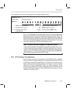
If either of bits 8 or 9 are set, then the reference oscillator enable is considered
set. This enables the PLL circuitry to regulate to the reference frequency, 32
kHz (assuming the idle state clock control is clear). Whichever state the
reference oscillator is in before idle, it remains in that state (running or stopped)
after idle. If the reference oscillator is left running during sleep, however, it
comes at a cost to power consumption. (This may be a necessary cost if, in
your application, elapsed time needs to be monitored during sleep.)
The power consumed during sleep when the RTO oscillator is left running is
greater than the power consumed during sleep when the CRO oscillator is left
running.
If the idle state clock control is clear, then the PLL circuitry, active during sleep,
will attempt to regulate the MC to whatever frequency is programmed in the
PLL multiplier (see Section 2.9.3, Clock Speed Control Register). The MC con-
tinues to run at this frequency, even during sleep, provided that the reference
oscillator is enabled.
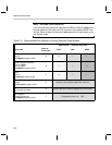
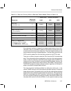
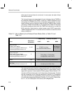
If the idle state clock control is set, then neither the MC, CPU clock, nor the
TIMER clocks run during sleep, unless the TIMER source is linked to the
reference oscillator (Section 2.8, Time Registers). These relationships are
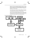
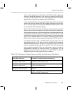
shown explicitly, as a function of the reduced power mode, in Table 2–4.
Because the DAC circuitry is the single most source of power consumed on
the C6xx, it is important to disable the DAC entirely before engaging any IDLE
instruction. This is accomplished at the DAC control register, address 0x34.
Refer to Section 3.2.2, DAC Control and Data Registers.
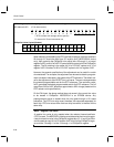
The ARM bit is another important control to consider before engaging the
reduced power mode. It is recommended that the ARM bit be cleared
whenever the idle state clock control is clear, and set whenever the idle state
clock control is set. The set ARM bit causes an asynchronous response to all
programmable interrupts when in the sleep state. (The cleared ARM bit yields
the standard synchronous response at all times.) Affected interrupts include
those tied to TIMER1 and TIMER2, as well as those tied to the inputs at Ports
F, D
2
, D
3
, D
4
, and D
5
. The advantage to having the ARM bit set is that the
device may be awakened by one of these interrupts, even when the PLL clock
circuitry is stopped in sleep (by virtue of the idle state control). The
disadvantage of the asynchronous response, however, is that it can render
irregularities in the timing of response to these same inputs.


