


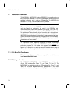

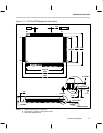
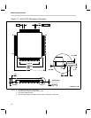
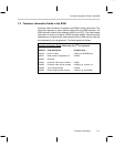
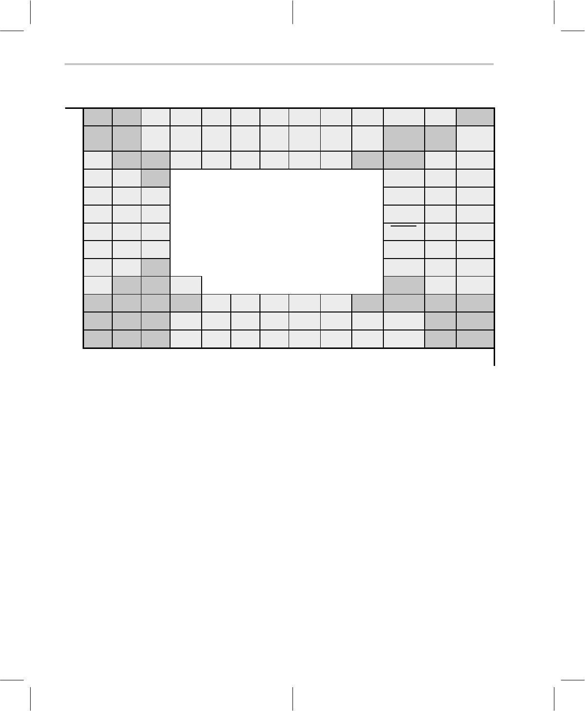
Mechanical Information
7-10
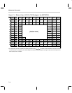
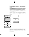
Figure 7–4. Bottom View of 120-Pin PGA Package of the MSP50P614
N
nc nc
†
V
DD
PF
7
PF
5
PF
2
V
PP
PG
15
PG
12
PG
10
V
SS
V
DD
nc
M
nc nc DAC
M
DAC
P
PF
6
PF
3
PF
1
PG
14
PG
11
PG
8
nc nc PG
7
L
PD
0
nc nc
†
V
SS
V
DD
PF
4
PF
0
PG
13
PG
9
nc nc PG
5
PG
4
K
PD
3
PD
1
nc PG
6
PG
3
PG
1
J
PD
5
PD
4
PD
2
PG
2
PG
0
scanout
H
V
DD
PD
7
PD
6
(b tt i )
pgmpuls SYNC scanclk
G
V
SS
PC
1
PC
0
(b
o
tt
om v
i
ew
)
RESET scanin PE
7
F
PC
2
PC
3
PC
4
PE
4
PE
5
PE
6
E
PC
5
PC
6
nc PE
0
PE
2
PE
3
D
PC
7
nc nc extra nc V
SS
PE
1
C
nc nc nc nc PB
1
PB
5
V
SS
PA
3
PA
7
nc nc nc nc
B
nc nc nc PB
0
PB
3
PB
6
PA
0
PA
2
PA
5
PLL OSC
OUT
nc nc
A
nc nc nc PB
2
PB
4
PB
7
V
DD
PA
1
PA
4
PA
6
OSC
IN
nc nc
1 2 3 4 5 6 7 8 9 10 11 12 13
†
It is important to provide a separate decoupling capacitor for the V
DD
, V
SS
pair which services the DAC. These pins are PGA
numbers N3 and L4, respectively. The relatively high current demands of the digital-to-analog circuitry make this a requirement.
Refer to section 6.1 for details.