Instruction Classification
4-25Assembly Language Instructions
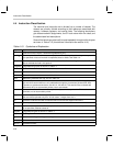
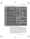
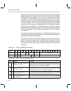
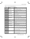
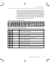
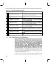
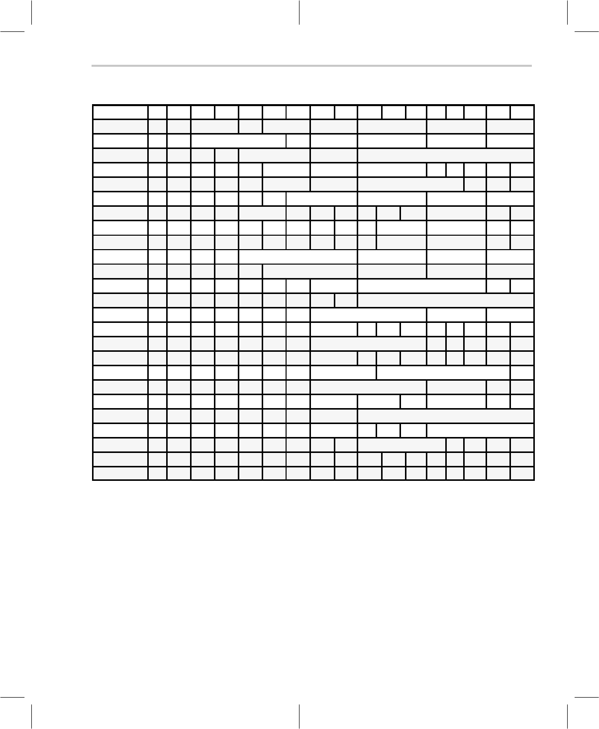
Table 4–12. Classes and Opcode Definition
Bit 16 15 14 13 12 11 10 9 8 7 6 5 4 3 2 1 0
Class 1a 0 0 C1a ~A~ next A An am Rx pm
Class 1b 0 1 C1b s An am Rx pm
Class 2a 1 0 1 0 C2a An imm8
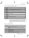
Class 2b 1 1 1 0 0 next A An C2b 0 0 1 A~ ~A
Class 3 1 1 1 0 0 next A An C3 0 A~
†
~A
Class 4a 1 1 1 1 0 C4a R am Rx pm
Class 4b 1 0 1 1 C4b k4 k3 k2 k7 k6 k5 R k1 k0
Class 4c 1 1 1 1 1 1 1 0 0 0 C4c R x x
Class 4d 1 1 1 1 1 1 1 0 0 1 C4d R x x
Class 5 1 1 0 1 C5 am Rx pm
Class 6a 1 1 0 0 C6a port4 am Rx pm
Class 6b 1 1 1 0 1 1 s An port6 C6b ~A~
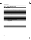
Class 7a 1 1 1 1 1 1 1 0 1 vector8
Class 7b 1 0 0 0 0 0 Not cc rx pm
JMP *An 1 0 0 0 1 0 x An x x x x x x x x
Class 7c 1 0 0 0 0 1 Not cc x x x x x
CALL *An 1 0 0 0 1 1 x An x x x x x x x x
Class 8a 1 0 0 1 1 flg n C8a flagadrs g/r
Class 8b 1 0 0 1 0 flg Not cc Rx C8b C8b
Class 9a 1 1 1 0 1 0 0 An C9a 0 Rx 1 1
Class 9b 1 1 1 1 1 1 0 C9a k
Class 9c 1 1 1 1 1 0 1 An 0 C9c x imm5
Class 9d 1 1 1 1 1 1 1 1 0 C9d 0 0 0 0
ENDLOOP n 1 1 1 1 1 1 1 1 0 0 0 0 1 0 0 0 n
NOP 1 1 1 1 1 1 1 1 1 1 1 1 1 1 1 1 1
†
Meaning of this bit depends on what class 3 instruction is used.
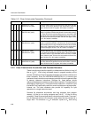
4.4.1 Class 1 Instructions: Memory and Accumulator Reference
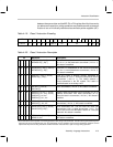
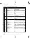
This class of instructions controls execution between data memory and the
accumulator block. In addition to the explicit opcode field that specifies an
arithmetic operation, an eight-bit data memory addressing mode reference
field (am, Rx, pm i.e., adrs field) controls the addressing of one input operand,
and a 4-bit field (An and next A in class 1a) or 2-bit field (An in class 1b) selects
an accumulator location as the other input operand. The results are written to
the addressed accumulator location (or to the offset accumulator in class 1a
if ~A bit = 1). In addition, each instruction can be treated as a single word length
operation or as a string, depending on the string control encoded in the op code
(s = 1 in class 1b and An = 11 binary in class 1a).


