


2-1
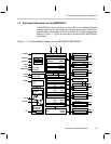
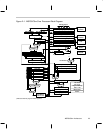
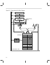
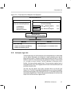
MSP50C6xx Architecture
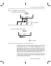
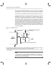
A detailed description of the MSP50C6xx architecture is included in this chap-
ter. After reading this chapter, the reader will have in-depth knowledge of inter-
nal blocks, memory organization, interrupt system, timers, clock control mech-
anism, and various low power modes.
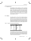
Topic Page
2.1 Architecture Overview 2–2. . . . . . . . . . . . . . . . . . . . . . . . . . . . . . . . . . . . . . . . .
2.2 Computation Unit 2–5. . . . . . . . . . . . . . . . . . . . . . . . . . . . . . . . . . . . . . . . . . . . .
2.3 Data Memory Address Unit 2–11. . . . . . . . . . . . . . . . . . . . . . . . . . . . . . . . . . .
2.4 Program Counter Unit 2–14. . . . . . . . . . . . . . . . . . . . . . . . . . . . . . . . . . . . . . .
2.5 Bit Logic Unit 2–14. . . . . . . . . . . . . . . . . . . . . . . . . . . . . . . . . . . . . . . . . . . . . . .
2.6 Memory Organization: RAM and ROM 2–15. . . . . . . . . . . . . . . . . . . . . . . .
2.7 Interrupt Logic 2–22. . . . . . . . . . . . . . . . . . . . . . . . . . . . . . . . . . . . . . . . . . . . . .
2.8 Clock Control 2–26. . . . . . . . . . . . . . . . . . . . . . . . . . . . . . . . . . . . . . . . . . . . . . .
2.9 Timer Registers 2–31. . . . . . . . . . . . . . . . . . . . . . . . . . . . . . . . . . . . . . . . . . . . .
2.10 Reduced Power Modes 2–33. . . . . . . . . . . . . . . . . . . . . . . . . . . . . . . . . . . . . .
2.11 Execution Timing 2–40. . . . . . . . . . . . . . . . . . . . . . . . . . . . . . . . . . . . . . . . . . .
Chapter 2