Functional Description for the MSP50C614
1-5Introduction to the MSP50C6xx
1.4 Functional Description for the MSP50C614
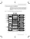
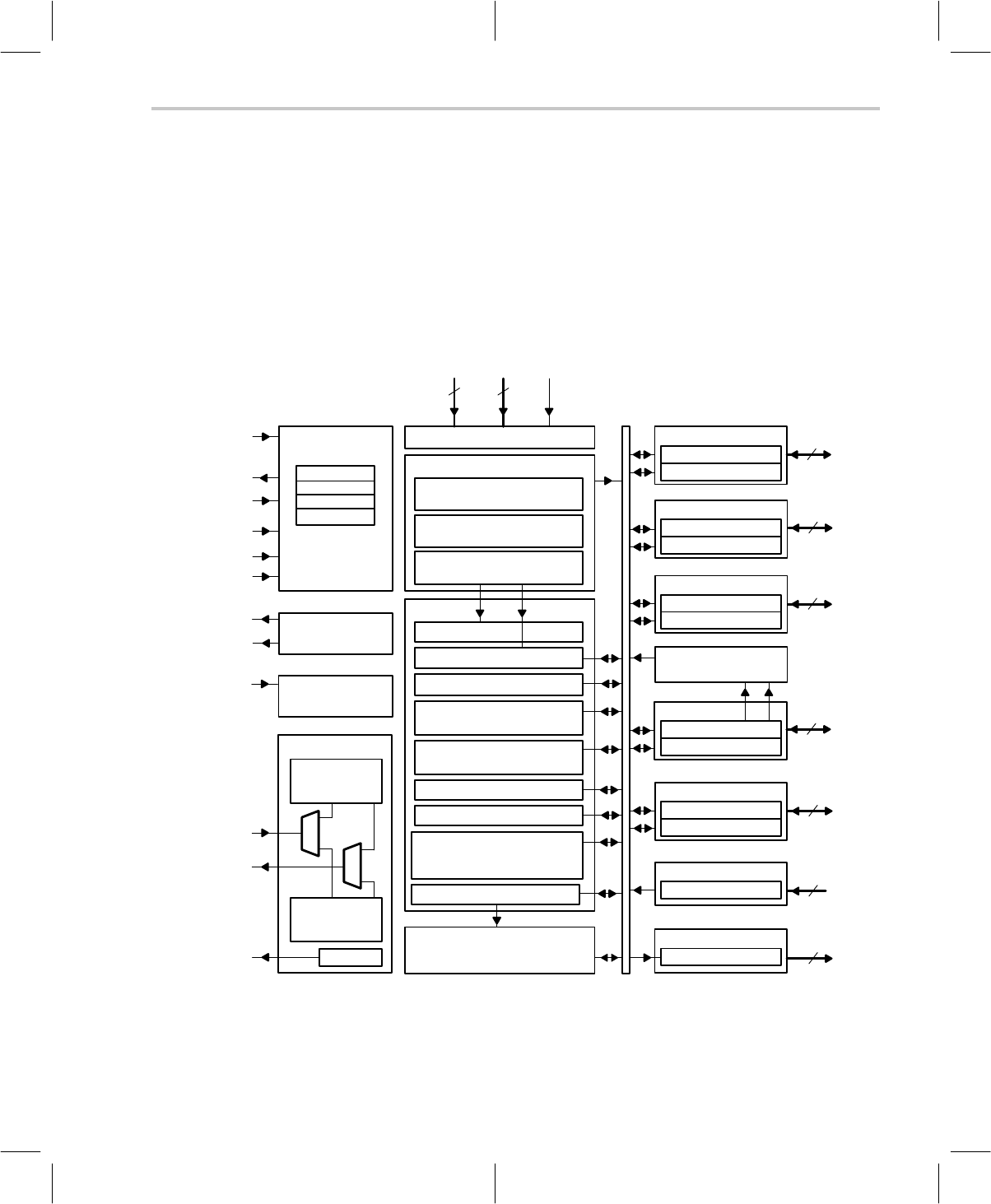
The MSP50C614 device consists of a micro-DSP core, embedded program
and data memory, and a self-contained clock generation system. General-pur-
pose periphery is comprised of 64 bits of flexible I/O. The block diagram ap-
pearing in Figure 1–1 gives an overview of the MSP50C614/MSP50P614
functionality.
Figure 1–1. Functional Block Diagram for the MSP50C614/MSP50P614
SCANIN
SYNC
PLL
OSCOUT
OSCIN
RESET
DACM
DACP
PGMPULSE
TEST
SCANCLK
SCANOUT
Serial Comm.
OTP Program
Emulation
Break Point
(C6xx only)
(P614 only)
DAC 0x30
32 Ohm PDM
Initialization
Logic
OSC Reference
Resistor
Trimmed
32 kHz nominal
Crystal
Referenced
32.768 kHz
PLL Filter
or
or
Scan Interface
Power (P614 only)
V
DD
V
PP
V
SS
55
(EP)ROM 32k x (16 + 1) bit
Test-Area
(reserved)
0x0000 to
0x07FF
User ROM 0x0800 to
0x7FEF
INT vectors 0x7FF0 to
0x7FFF
Core
Instr. Decoder
PCU Prog. Counter Unit
CU Computational Unit
TIMER1 PRD1
0x3A
TIM1
0x3B
TIMER2
PRD2
0x3E
TIM2
0x3F
Clock Control
0x3D
Gen. Control
0x38
Interrupt Processor
FLAG
0x39
MASK
0x38
DMAU
Data Mem. Addr.
RAM 640 x 17 bit
(data)
0x000 to
0x027F
A port I/O
Data 0x00
Control 0x04
B port I/O
Data 0x08
Control 0x0C
C port I/O
Data 0x10
Control 0x14
Comparator
1 bit: PD
5
vs PD
4
D port I/O
Data 0x18
Control 0x1C
E port I/O
Data 0x20
Control 0x24
F port INPUT
Data 0x28
G port OUTPUT
Data 0x2C
8
PA0–7
8
PB0–7
8
PC0–7
8
PD0–7
8
PE0–7
8
PF0–7
16
PG0–15
+ –


