


I/O
3-2
3.1 I/O
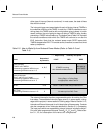
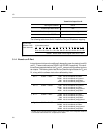
This section discusses the I/O capabilities of the MSP50C6xx family. The fol-
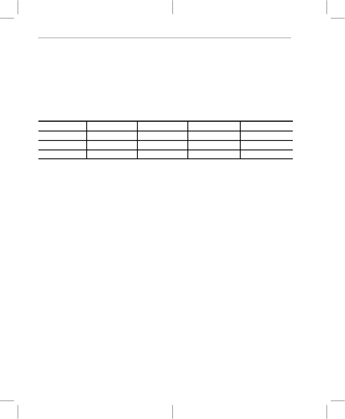
lowing table shows the number and types of I/O available on each device.
Please note that this section discusses all I/O ports, which are only available
on the MSP50C614 device. All other devices have only a subset of the I/O that
is available on the MSP50C614.
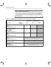
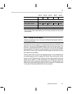
Device Ports Available
No. of General
Purpose I/O
No. of Dedicated
Inputs
No. of Dedicated
Outputs
MSP50C614
A,B,C,D,E,F,G 40 8 16
MSP50C604 C,D 16 0 0
MSP50C605 C,D,E,F 24 8 0
MSP50C601 C,D,E,F 24 8 0
3.1.1 General-Purpose I/O Ports
The forty configurable input/output pins are organized in 5 ports, A,B,C,D, and
E. Each port is one byte wide. The pins within these ports can be individually
programmed as input or output, in any combination. The selection is made by
clearing or setting the appropriate bit in the associated control register (Control
A, B, C, D, or E). Clearing the bit in the control register renders the pin as a
high-impedance input. Setting the control bit renders the pin as a totem-pole-
output.
When configured as an input, the data presented to the input pin can be read
by referring to the appropriate bit in the associated data register (Data A, B,
C, D, or E). This is done using the IN instruction, with the address of the data
register as an argument.
When configured as an output, the data driven by the output pin can be
controlled by setting or clearing the appropriate bit in the associated data
register. This is done using the OUT instruction, with the address of the data
register as an argument.