


AMD Confidential
User Manual November 21
st
, 2008
Chapter 7: Device Configuration 59
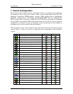
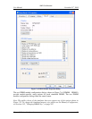
7.3 DIMM Device
The DIMM device provides a simulation model of an array of up to four dual-inline-
memory modules (DIMMs). The model provides RAM storage and serial presence detect
(SPD) ROM access for each DIMM. Bytes 0, 5, 13, and 31 (zero-based) of the SPD data
are used to configure the DIMM model. The remaining SPD entries are available for
BIOS probing, but are not used to configure the DIMM model.
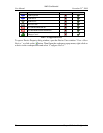
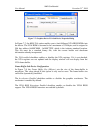
The RAM array for each DIMM is sized based on parameters contained in the SPD array.
SPD array bytes 5 and 31 are used to calculate the size of the DIMM's RAM array. If
byte 0 in the SPD array has a value of zero, then the DIMM device does not respond to
any SMBUS read attempts on the module. This indicates to the reading device that an
SPD ROM is not available on the DIMM module. By appropriately setting bytes 5 and
31, and clearing byte 0, the model simulates a valid DIMM that contains no SPD ROM.
Dual data rate (DDR) DIMMs use bidirectional data strobe signals to latch data on
transfers. The Northbridge device contains Programmable Delay Lines (PDLs) that are
used to delay the Data Qualification Signal (DQS) signals so that the edges are centered
on the valid data window. BIOS algorithms are used to locate the valid data window and
adjust the PDLs accordingly.
Physical DIMMs provide 8 bytes of data per access. On the module, the 8 bytes of data
are stored across several memory devices. The data width of the memory devices on the
DIMM (SPD byte 13) determines how many PDLs are used. DIMMs that use 8-bit or 16-
bit memory devices use one PDL per byte of width (eight total PDLs). DIMMs that use
4-bit devices use one PDL per nibble (16 total PDLs).
The memory controller in the AMD Opteron™ processor includes two DDR channels
that are ganged into a single effective 128-bit interface. Each access to memory hits a pair
of 64-bit DIMMs, where one DIMM supplies the lower 64 bits while the other DIMM
supplies the upper 64 bits. Each DIMM must have the same arrangement in size and
number of banks.
For each valid access to DRAM, the memory controller will assert one of eight bank-
select lines (CS7:0). Each bank-select line selects one “virtual bank.” A virtual bank is
the combination of one bank on the lower DIMM, and the corresponding bank on the
upper DIMM. Row and column addresses select the data offset within the virtual bank.