


AMD Confidential
User Manual November 21
st
, 2008
64 Chapter 7: Device Configuration
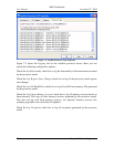
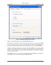
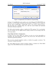
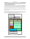
The upper part of the dialog lists some summary information. This information, which is
derived from the SPD data, gives a quick indication of the type of device being
simulated.
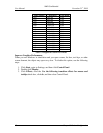
The center section of the dialog lists all 256 bytes of data held in the simulated SPD
ROM. The list box provides a description of each byte index in the ROM. If a description
is selected, the corresponding data byte is displayed in the text box to the right.
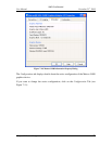
The Import SPD and Export SPD buttons provide the option of loading and saving SPD
ROM data. The file format is an unformatted binary image, with an extension of “*.spd”.
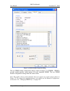
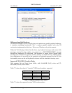
The bottom section of the dialog is used to configure DDR PDL Response ranges for the
simulated DIMM. PDL response ranges can be individually set for each of 16 PDLs.
Adjusting the Low and High value modifies the response range for a particular PDL.
When an appropriate response range is set for one PDL, the same range can be applied to
all 16 PDLs by clicking on the Match PDLs button. The Reset PDLs button sets all 16
PDL response ranges to their maximum range (0 - 255).
Log Messages
This device does not produce log messages.
Difference from Real Hardware
The DIMM device does not simulate timing-related issues except for PDL error
simulation. The performance of real DIMM hardware is highly dependent on timing and
loading issues.
ECC simulation is not provided.