ML361 Virtex-II Pro Memory Board www.xilinx.com 11
UG060 (v1.2) November 8, 2007
R
Chapter 1
Introduction
Overview
The ML361 Virtex-II Pro DDR400/PC3200 Memory Board provides a communications
platform between a Virtex-II Pro FPGA and high-speed double-data-rate (DDR) memories
with operating speeds up to 200 MHz. The ML361 has three major functions:
• Tests and verifies the interoperability of Virtex-II Pro devices with high-speed DDR
memories
• Serves as a development platform for Xilinx and its customers to use for building
memory controllers
• Provides a means by which Xilinx can demonstrate high-speed DDR memory
interoperability
This document describes the functional blocks within the ML361. It also provides various
recommendations and requirements for usage of the board, including electrical
requirements, logic analyzer requirements, and signal integrity issues. Simulation results
using IBIS also are included.
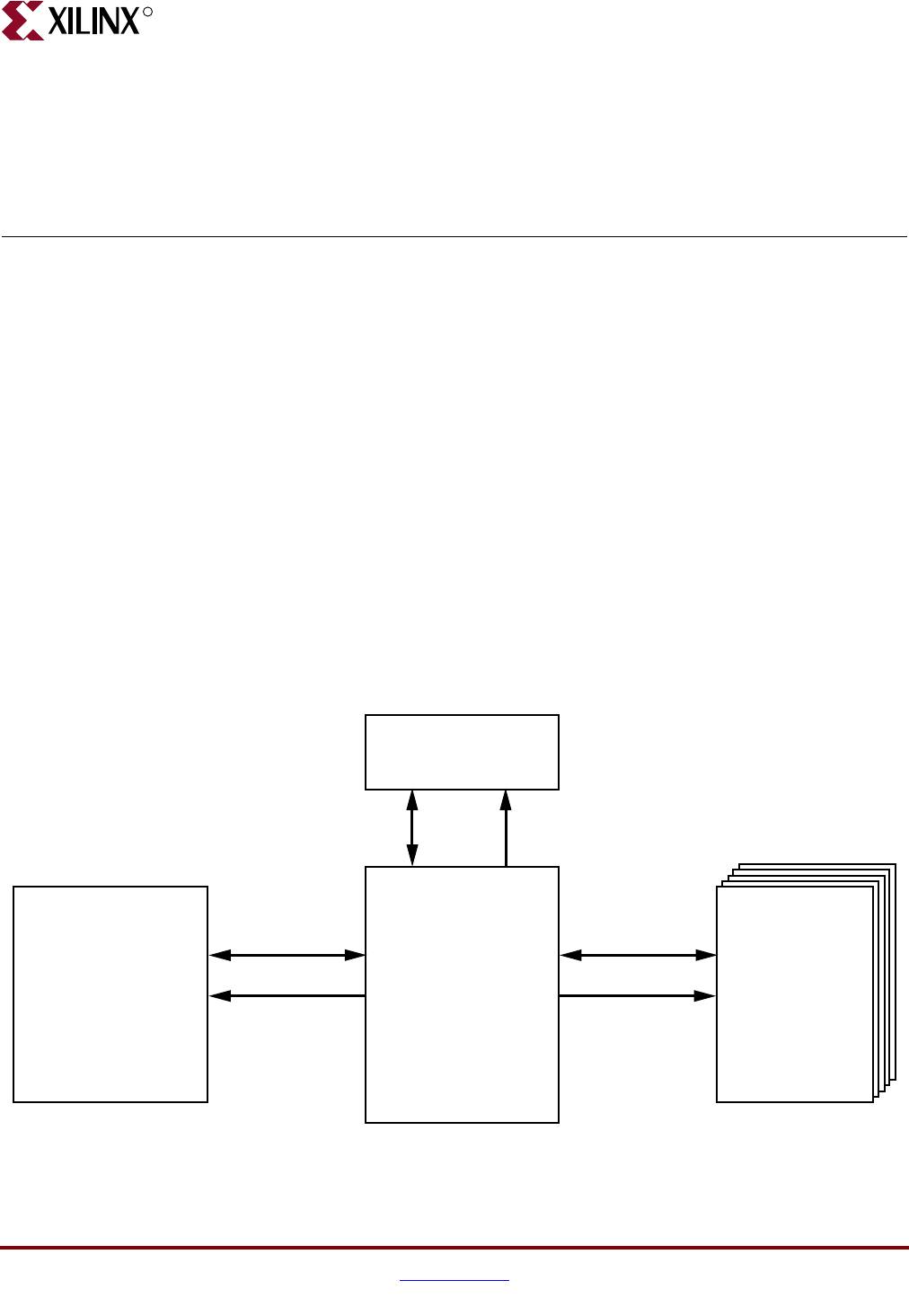
Figure 1-1 shows a simplified block diagram of the ML361 memory interfaces.
X-Ref Target - Figure 1-1
Figure 1-1: Simplified Block Diagram of Memory Board Interfaces
Virtex-II Pro FPGA
XC2VP20FF1152-6
DDR SDRAM
(MT46V32M8TG-5B)
Data (72 bits)
Data (8 bits)
Address/Control
Address/Control
Data (72 bits)
Address/Control
DDR
SDRAM DIMM
128MB
(MT4VDDT1664-AG-40BC3)
DDR
SDRAMs
256Mb
(4 MT46V16M16TG-5B
and
1 MT46V32M8TG-5B)
ug060_c1_01_012104


