30 www.xilinx.com ML361 Virtex-II Pro Memory Board
UG060 (v1.2) November 8, 2007
Chapter 4: Signal Integrity Recommendations and Simulations
R
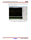
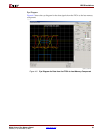
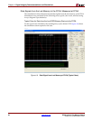
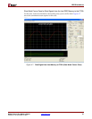
c. Address and Control Signals
- Address and Control Signals with 45
Ω Transmission Lines Measured at First
DDR Component (Typical)
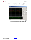
- Address and Control Signals with 55
Ω Transmission Lines Measured at First
DDR Component (Typical)
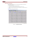
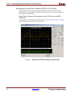
Notes on the Simulation Results
The provided screen captures show the results of each simulation. The signals in these
screen captures are color-coded as follows:
• Red signal – at FPGA
• Yellow signal – at memory
The two horizontal yellow lines are V
ref
± 100 mV where V
ref
=1.3 V.


