ML361 Virtex-II Pro Memory Board www.xilinx.com 57
UG060 (v1.2) November 8, 2007
IBIS Simulations
R
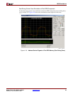
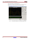
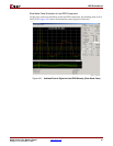
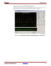
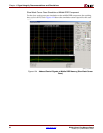
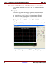
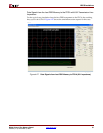
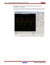
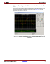
Data Signals from the Last DDR Memory to the FPGA with 55Ω Transmission Line
Impedance
For the typical case simulation from the last DDR component to the FPGA, the resulting
duty cycle is 46.4/52.62. Figure 4-27 shows the simulation screen capture for this case.
X-Ref Target - Figure 4-27
Figure 4-27: Data Signals from Last DDR Memory to FPGA (55Ω Impedance)
ug060_c5_27_031204


