22 www.xilinx.com ML361 Virtex-II Pro Memory Board
UG060 (v1.2) November 8, 2007
Chapter 3: Electrical Requirements
R
FPGA Internal Power Budget
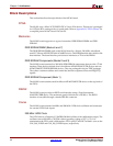
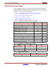
The following tables show the power consumption values inside the FPGA based on the
complete DDR design. These results are derived using the Xilinx Power Estimator tool.
Block Select RAM, Block Multiplier, Processor, and MGT Power tables are not included in
this section as they are not used in this application.
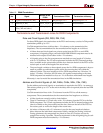
• Table 3-2, “XC2VP20FF1152 Estimated Power Consumption,” page 22
• Table 3-3, “XC2VP20FF1152 Temperature Specifications,” page 22
• Table 3-4, “Device Quiescent Power,” page 22
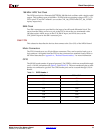
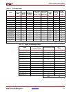
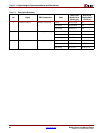
• Table 3-5, “CLB Logic Power,” page 23
• Table 3-6, “Digital Clock Manager Power,” page 23
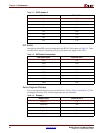
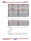
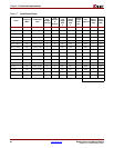
• Table 3-7, “Input/Output Power,” page 24
Table 3-2: XC2VP20FF1152 Estimated Power Consumption
Parameter Value Units
Total Estimated Design Power 6873 mW
Estimated Design VCC
INT
1.5 V Power 3811 mW
Estimated Design VCC
AUX
2.5 V Power 417 mW
Estimated Design VCCO 3.3 V Power 0 mW
Estimated Design VCCO 2.5 V Power 2645 mW
Estimated Design VCCO 1.8V Power 0 mW
Estimated Design VCCO 1.5 V Power 0 mW
Estimated Design VCCO 1.2 V Power 0 mW
Estimated Design VCC
AUX
RX 2.5 V Power 0 mW
Estimated Design VCC
AUX
TX 2.5 V Power 0 mW
Estimated Design VT
RX
2.5 V Power 0 mW
Estimated Design VT
TX
2.5 V Power 0 mW
Table 3-3: XC2VP20FF1152 Temperature Specifications
Parameter Value Units
Ambient Temperature 25 •C
Air Flow 0 LFM
Junction Temperature 107 •C
Table 3-4: Device Quiescent Power
VCC
INT
Subtotal (mW) VCC
AUX
Subtotal (mW)
450 417


