ML361 Virtex-II Pro Memory Board www.xilinx.com 71
UG060 (v1.2) November 8, 2007
R
Appendix B
FPGA Pinout
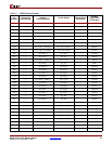
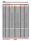
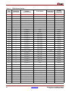
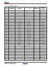
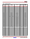
Table B-1 summarizes the pinout of the XC2VP20FF1152-6 FPGA in the ML361 board. The
slice coordinates mentioned in Table B-1 refer to the RPM grid coordinates corresponding
to the respective I/O pin location. I/O pin names marked as GND refer to unused I/Os
that are directly connected to GND. I/O pin names marked as PULLDOWN refer to
unused I/Os that are connected to GND through a zero ohm resistor. The 0
Ω resistor can
be removed to use the corresponding I/O for any test purposes.
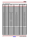
Table B-1: FPGA Pinout
Pin
Numbers
Virtex-II Pro
Bank Number
Package
Functional Name
I/O Pin Names
Internal Script
Information
Package
Flight Times
(in microns)
U23 7 VCCO_7
E29 0 IO_L01N_0/VRP_0 RXD 11097.26
E28 0 IO_L01P_0/VRN_0 TXD 10150.32
H26 0 IO_L02N_0 resetN 6327.18
G26 0 IO_L02P_0 DIP1 7905.95
H25 0 IO_L03N_0 DIP2 5691.71
G25 0 IO_L03P_0/VREF_0 DIP3 6996.94
J25 0 IO DIP4 5273.75
K24 0 IO_L06N_0 DIP5 3344.34
J24 0 IO_L06P_0 DIP6 4601.94
F26 0 IO_L07N_0 DIP7 9207.2
E26 0 IO_L07P_0 DIP8 10718.03
D30 0 IO_L08N_0 GPIO08 15834.96
D29 0 IO_L08P_0 GPIO09 14848.81
K23 0 IO_L09N_0 GPIO10 3066.04
J23 0 IO_L09P_0/VREF_0 GPIO11 4323.64
H22 0 IO_L37N_0 GPIO12 4727.82
G22 0 IO_L37P_0 GPIO13 5923
D26 0 IO_L38N_0 GPIO14 15218.77
C26 0 IO_L38P_0 GPIO15 15469.57


