ML361 Virtex-II Pro Memory Board www.xilinx.com 9
UG060 (v1.2) November 8, 2007
R
Preface
About This Guide
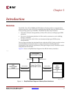
This document describes the design of the ML361 Virtex-II Pro™ DDR400/PC3200
Memory Board, which connects a Virtex-II Pro FPGA to DDR memories.
Guide Contents
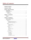
This manual contains the following chapters:
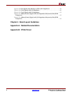
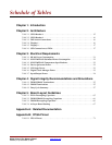
• Chapter 1, “Introduction,” describes the purpose of the ML361 board and provides its
key features.
• Chapter 2, “Architecture,” provides a block diagram of the memory board and
describes the key components.
• Chapter 3, “Electrical Requirements,” lists the electrical specifications for the memory
board.
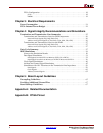
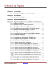
• Chapter 4, “Signal Integrity Recommendations and Simulations,” provides
information on termination, transmission lines, and duty cycles. It also gives the
results of several IBIS simulations.
• Chapter 5, “Board Layout Guidelines,” provides information on decoupling
capacitors, ground signals, and PCB layout.
• Appendix A, “Related Documentation,” lists data sheet and external website
references specific to the ML361 components.
• Appendix B, “FPGA Pinout,” provides the pinout of the Virtex-II Pro FPGA.
Additional Resources
For additional information, go to http://support.xilinx.com. The following table lists
some of the resources you can access from this website. You can also directly access these
resources using the provided URLs.
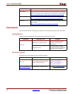
Resource Description/URL
Tutorials Tutorials covering Xilinx design flows, from design entry to verification
and debugging
http://support.xilinx.com/support/techsup/tutorials/index.htm
Answer Browser Database of Xilinx solution records
http://support.xilinx.com/xlnx/xil_ans_browser.jsp
Application Notes Descriptions of device-specific design techniques and approaches
http://support.xilinx.com/apps/appsweb.htm


