ML361 Virtex-II Pro Memory Board www.xilinx.com 13
UG060 (v1.2) November 8, 2007
R
Chapter 2
Architecture
This chapter provides functional descriptions of the major blocks within the ML361 board
design. For more detailed information on the design, refer to the schematics, which are
located at http://www.xilinx.com/bvdocs/userguides/ug060.zip
.
ML361 Board Block Diagram
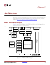
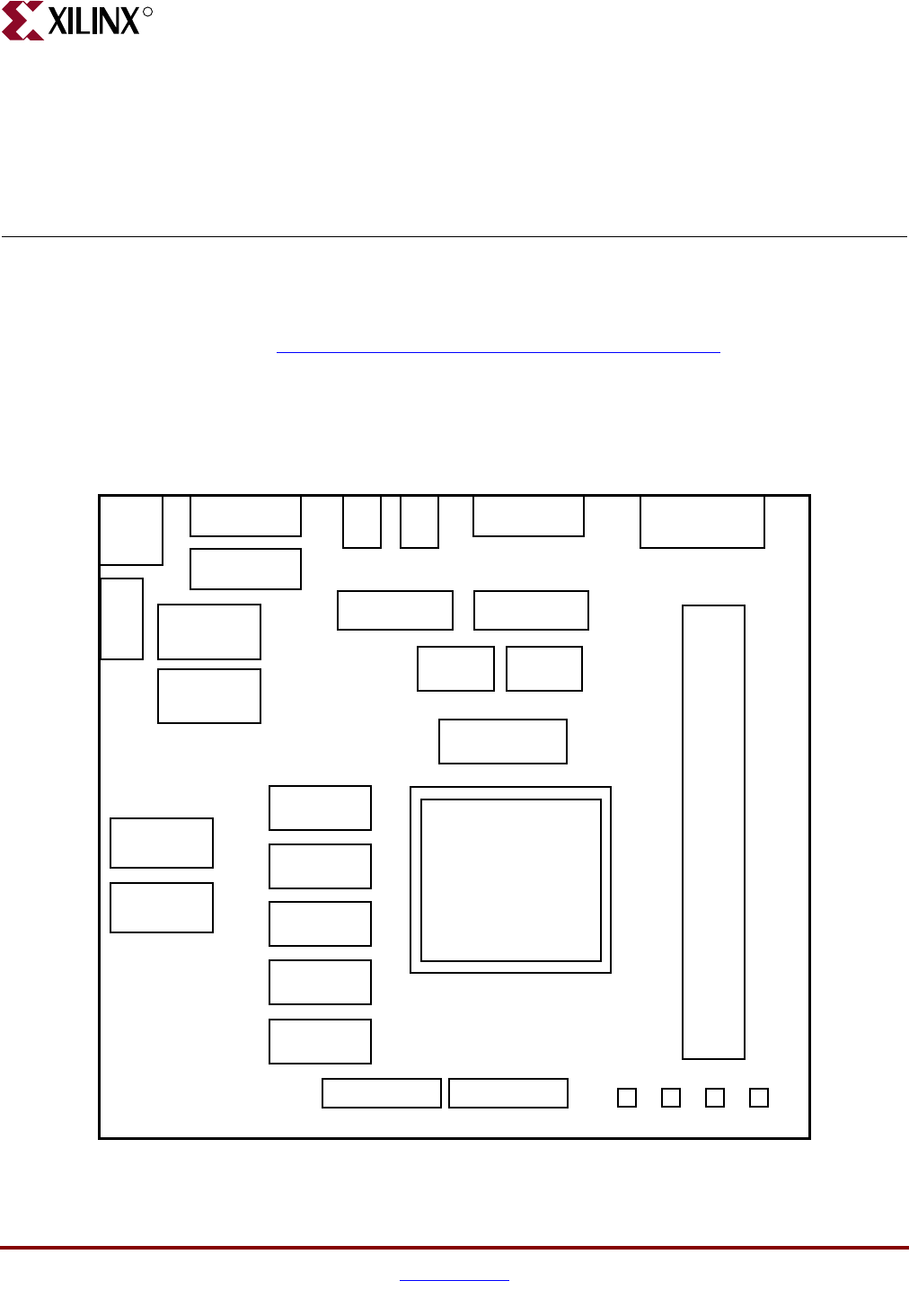
Figure 2-1 shows a block diagram of the ML361 board. Refer to the following section for
additional information on the major blocks.
X-Ref Target - Figure 2-1
Figure 2-1: ML361 Board Block Diagram
ug060_c2_01_121703
Switch
5V
Input
Jack
3.3V Regulator
(5.5A)
2.6V Regulator
(10A)
1.3V Regulator
(5.5A)
2.6V Regulator
(10A)
JTAG Port
Serial Port
DIP Switch
PROM
CLOCK
(166 MHz)
CLOCK
(200 MHz)
DDR SDRAM
(x16)
DDR
SDRAM
DIMM
(x64)
DDR SDRAM
(x16)
DDR SDRAM
(x16)
DDR SDRAM
(x16)
DDR SDRAM
(x8)
DDR SDRAM
(x8)
MICTOR (38-pin) MICTOR (38-pin)
Push1 Push2 Prgm Reset
XC2VP20FF1152C-6
GPIO Header GPIO Header
7-Segment Displays


